Published on September 7, 2015
A+Augmenter la taille du texteA-Réduire la taille du texteImprimer le documentEnvoyer cette page par mail
from November 1, 2015 to August 31, 2016
|
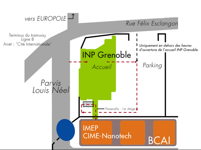
Access map
Job period :
Position open from September 1st 2015
1 year post-doctoral position
Subject:
Development of an Impulse Radio emitter for Ultra Wide Band applications
Context:
Impulse Radio Ultra Wide Band (IR-UWB) is an emerging technique for wireless communications which has demonstrated its interest in terms of bit rates, power consumption and specific absorption rate. Many architectures of IR-UWB emitters have been developed and published whose one is based on pulse synthesis. Although this method leads to complex transmitters, it is theoretically able to cover all the channels introduced by IEEE 802.15.4 and IEEE 802.15.6 standards. Thus, a design of this of IR-UWB emitters, which is composed of an analog core and high speed logic functions, has been developed and partially implemented in a 65nm technology.
Plan:
The first task is to transpose the analog core of the synthesizer, which has been already implemented in a 65nm technology, to a 28nm FD-SOI technology. Performances have to be estimated with the help of post-layout simulations and compare with the ones previously obtained.
The second task consists in the design of high speed logic functions which are necessary to drive synchronously the analog core. Some functions have already been sized in a 65nm technology but many functions need to be implemented yet in a 65nm technology. Finally, these functions will be designed in a 28nm FD-SOI technology too.
The both tasks will lead to the realization of one test chip at least.
Applicant profile:
The applicant must have a Ph.D degree, or a Master degree with an experience of 3 years in microelectronic. He must have skills in integrated-circuits design from electrical simulations to post-layout validations. Knowledge of 65nm and 28nm FD-SOI technologies from STMicroelectronics and of mixed-signal simulations will be appreciated.
A+Augmenter la taille du texteA-Réduire la taille du texteImprimer le documentEnvoyer cette page par mail
Date of update October 21, 2015
Nos sites
eServices


