Aller au menu Aller au contenu
Microelectronics, electromagnetism, photonics , microwave

> Research > CMNE > Ultimate CMOS

Ultimate CMOS and Alternative Technologies

Headed by : Gérard GHIBAUDO

Context and Objectives

The « Ultimate CMOS » group has a 35 year experience in the design and characterization of semiconductor devices. In particular, it has been playing a pioneering role in the study and promotion of CMOS technologies on SOI. Our mission consists in exploring and expanding the frontiers of CMOS micro- and nano-electronics. The permanent objective is to unveil the physical mechanisms involved and their exploitation for the development of technologies, devices and their applications.

Our research activities are partly developed within the framework of the Labex MINOS in Minatec, in strong link with our local partners (CEA, ST, SOITEC…) and international collaborators (European networks of excellence, projects and bilateral agreements…). They are widely supported by European and national projects).

New materials and new MOS architectures:
Being convinced that SOI and its variants are the key of future CMOS expansion and of the transition from micro to nanoelectronics, we are devoting much effort to this subject, both at the level of materials and devices. We are for instance studying alternative materials to bulk silicon such as SOI, GeOI, strained SiGe and III-V materials integrated on silicon, or wide bandgap materials. We are also studying the potential of new concepts and new architectures of transistors and memories. Steep subthreshold slope devices are for instance targeted for applications combining performance and low power consumption.

Keywords: SOI, ultra-thin body and BOX (UTBB), GeOI, multiple gates, nanowire (NW), III-V MOSFET, Tunnel FET, steep slope, floating body effects, ReRAM, NVM, statistical and dynamic variability…

Experimental analysis of electron transport and interfaces:
Our core expertise in characterization and parameter extraction is constantly solicited to transport properties and interface quality for new materials (used for channel, gate of buried oxide) or to study the influence of mechanical engineering and of device architecture (ultra-thin films, multiple gates, FinFETs, JLTs, nanowires, etc.). It is important to note that the conclusions about the suitability of a given material should always be driven for short channels typical of the envisioned technology nodes as they can be dramatically different from what is found for long channels!

Keywords: electron and hole mobility, electron and hole velocity, saturation velocity, thermal velocity, out-of-equilibrium transport, scattering mechanisms, ballistic transport, quantum confinement, quantum coupling, front/back channel coupling, volume inversion, interface traps, defects…

Characterization techniques and parameter extraction methodologies:
Understanding device physics requires that physically sounded parameters that are relevant to the mechanisms involved (such as electrostatic coupling, out-of-equilibrium and ballistic electron transport, scattering mechanisms, trapping/detrapping, or quantum effects) can be extracted from electrical characteristics (DC, small signal, transient or noise characteristics). To maintain our expertise at the best level, we are constantly developing our characterization techniques, the compact physical models that support our extraction methodologies as well as our simulation tools.

Keywords: pseudo-MOS, Y-function, split CV, G-? analysis, transient analysis, Hall measurements, channel magnetoresistance, charge pumping, low frequency noise (LFN), low temperature measurements…

Alternative technologies:
While this expertise has been initially been developed for CMOS, we are using it as well for the study of alternative technologies to silicon, which are presently attracting much attention, such as devices on wide bandgap materials (SiC, GaN), organic substrates or 2D materials.

Examples

Robust fabrication of suspended ribbons made of CVD graphene with scalable fabrication techniques

Graphene devices 
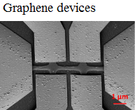
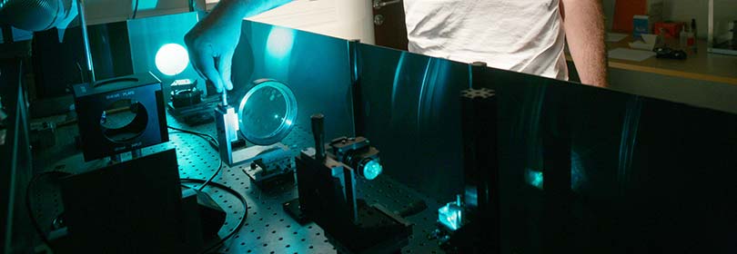
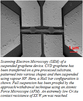
While it has been extensively proven that graphene was featuring many extraordinary properties that make it potentially interesting in a wide variety of fields, its full development will only be possible once scalable and robust fabrication routes compatible with large substrates will be available. This is a real challenge. Graphene growth by CVD on metal catalyst layer and its transfer to any type of substrate are first steps in this direction. However, processing such an ultra-thin layer of organic composition is not straightforward, with many issues to be solved, related for instance to capillary effects, control of ad-hesion, residual strain or incompatibility with some usual cleaning processes. We have succeeded in developing such a route for the fabrication of suspended structures. This opens the field to a variety of applica-tions, for instance in the field of NEMS.
Contact: Mireille MOUIS
Support and collaborations: CNRS network of technological facilities Renatech (clean rooms for device fabrication), Georg Düsberg’s team, Trinity College, Dublin (growth and transfer of CVD graphene)
See for instance: O. I. Aydin, T. Hallam, J.L. Thomassin, M. Mouis, and G. Duesberg, Challenges in Suspending CVD Graphene:More than Capillary Effects, 15th International Conference on Ultimate Integration on Silicon (ULIS), 8-9 April 2014, Stockholm, Sweden, IEEE, Proceedings of ULIS 2014, pp. 33-36, doi: 10.1109/ULIS.2014.6813899 (2014)

Channel magnetoresistance in the saturation regime of operation MOS transistors: a new insight into high field transport


Magnétoresistance de canal
It has been shown that channel magnetore-sistance, measured under transverse mag-netic field in the linear regime of operation (low VDS) of MOSFET transistors of wide and short geometry, could be used to ex-tract channel mobility (µMR) without being influenced by uncertainties on the exact value of channel length which is less pre-cisely known as device dimensions de-crease. We have recently shown that the B2 dependence of channel magnetoresistance is observed in the whole range of bias volt-ages, from linear regime to saturation (from low to high VDS). It can be used to extract an apparent mobility, which varies with gate and drain voltages. These variations are fully explained by a new physical compact model that we have developed, from which both linear mobility at low field and high field velocity can be extract-ed. When applied to 14nm FDSOI devices, this new method showed that high field operation was driven by out-of-equilibrium transport without being yet ballistic.
 
Contact : Gérard Ghibaudo, Mireille Mouis
Support and collaborations:  LCMI (high magnetic field), STMicroelectronics (devices pro-vision)
See for instance : Minju Shin, Ming Shi, Mireille Mouis, Antoine Cros, Emmanuel Josse, Ben-jamin Piot, Gyu-Tae Kim and Gérard Ghibaudo, Experimental and theoretical investigation of magnetoresistance from linear operation to saturation in 14nm FDSOI MOS devices, submit-ted to IEEE Transactions on Electron Devices, 2014
 ]
Simulation of gate capacitance variation
The split-CV method consists in analysing the gate to channel (CGC) and gate to sub-strate (CGB) capacitances variation with gate voltage (VG). It is a powerful method to extract physical information about elec-tron transport, charge control, or device physical characteristics (doping level, oxide thickness, etc.). However, when SOI substrates started to be used instead of bulk silicon, it became impossible to exploit CGB, due to buried oxide (BOX) thickness. We have shown that the emergence of ul-tra-thin BOX devices with backplane volt-age control could revive the method. By combining the full split CV technique with backplane voltage variation, we demon-strated that it was possible to extract physi-cal characteristics of the whole stack, from backplane to front gate. New parameters can be extracted while others are more directly evaluated and thus more reliable.

Contact : Gérard Ghibaudo, Mireille Mouis
Support and collaborations: CATRENE/Reaching22, ENIAC/Places2Be, in collaboration with STMicroelectronics (device provision)
See for instance :  Minju Shin, Ming Shi, Mireille Mouis, Antoine Cros, Emmanuel Josse, Gyu-Tae Kim and Gérard Ghibaudo, Full split C-V method for parameter extraction in Ultra Thin BOX FDSOI MOS devices, Solid-State Electronics, accepted 16 Apr. 2014, first published online 10 May 2014, doi: 10.1016/j.sse.2014.04.039 (May 2014).

Evolution of low frequency noise and noise variability through CMOS bulk technology nodes from 0.5 ?m down to 20 nm

We use low frequency noise (LFN) analysis as a non-destructive experimental tool to evaluate the quality of dielectric interfaces, which have a direct impact on electronic devices quality. Evaluating LFN behavior through several technology nodes can thus provide a global idea about device noise behavior and interface quality. Furthermore, CMOS scaling down is ac-companied by a reduction of device area, which subsequently leads to important issues related to statistical parameter variability. In this respect, LFN, which scales inversely with device area, is becoming a major concern not only for analog but also for digital circuits operation. In particular, LFN can limit the performance of VCO, DRAMs, SRAM cells, inverters and other mixed signal circuits. In addition, LFN is also subjected to variability due to device-to-device dispersion. This can also affect seriously integrated circuit functionality. For these reasons, it is required to study in detail LFN and its variability through CMOS technology nodes.
Evolution with scalling down of volumetric trap density
 
In this context, we carried out a thorough investigation of LFN and statistical noise variability through CMOS planar bulk technologies manufactured along the past 12 years and extended to the most recent 20 nm CMOS bulk technology node for the first time. The evolution with time and technology generation was studied by plotting oxide trap density Nt as a function of equivalent oxide thickness (EOT). It was found that Nt increased by almost two decades while EOT decreased from 12 nm (for the 0.5 ?m node) to 1.3 nm (for the 20 nm node) for n- and p-MOS. In spite of this trend, the LFN statistical variability has been surprisingly well controlled. It has even been improved for the 28 and 20 nm nodes.
Contact : Gérard Ghibaudo
Collaborations:  STMicroelectronics and CEA-LETI
See for instance : E. G. Ioannidis, S. Haendler, C. G. Theodorou, S. Lasserre,  C. A. Dimitriad-is, G. Ghibaudo, Evolution of low frequency noise and noise variability through CMOS bulk technology nodes from 0.5 ?m down to 20 nm, Solid State Electronics, 95, 28-31 (2014).

Low frequency noise variability

As device dimensions are scaling down, variability is increasing. This does not only concern dimensions, doping levels and static parameters but also dynamic parameters such as the low frequency noise (LFN). This has important implications as it can raise issues during device operation. The figure below shows how the statistical variability of LFN increases when device width decreases from 3µm to 60nm for the same technology (14nm node) and with the same number of dies included in the statistics (45 dies).
Increase of low frequency noise variability

Contact : Gérard Ghibaudo
Support and collaborations: STMicroelectronics. Projet ENIAC Places2Be
See for instance : E. G. Ioannidis, S. Haendler, C. G. Theodorou, S. Lasserre,  C. A. Dimitri-adis, G. Ghibaudo, Evolution of low frequency noise and noise variability through CMOS bulk technology nodes from 0.5 ?m down to 20 nm, Solid State Electronics, 95, 28-31 (2014).

Modeling basic charge pumping curves in various experimental conditions

Mdeling basic charge pumping curves 
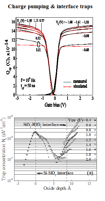
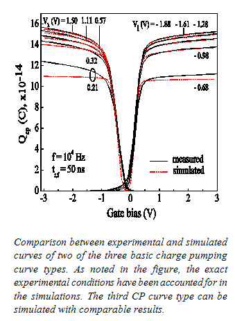
TheCharge pumping (CP) is a technique that applies on MOS transistors and allows the study of semiconductor-insulator interfaces traps. Depending on both, the specific CP technique used and the semiconductor-insulator studied, the mean interface trap density, the trap density vs. energy profile in the semiconductor bandgap, the traps capture cross-section or the trap density vs. insulator depth profile can be extracted. However, until recently, basic CP mecha-nisms were not correctly understood so that the three basic CP curve types had not been simulated satisfactorily. The figure shows two of these three basic curve types and their simulation. From the model that permitted these results, basic CP processes are validated along with the main Si-SiO2 interface traps properties introduced so that deeper studies of Si-SiO2 interface traps become possible.      
         
Contact : Daniel Bauza
Support: European network of Excellence NANOSIL, Catrene Project UTTERMOST. 
See for instance : D. Bauza, “On the meaning of charge pumping curve edges” International Reliability Physics Symposium (IRPS), April 14-18, 2013; Monterey, CA, USA, Proceedings pp. GD 2.1-2.4.; D. Bauza,“Charge pumping, an overview of the technique and recent new features,” Tutorial, 2011 IEEE International Integrated Reliability Workshop (IIRW) – Stanford Sierra Conf. Center - S. Lake Tahoe, CA, USA, October 16-20, 2011.      

The use of charge pumping for studying defects in high-k gate stacks.

Charge pumping and interface traps 
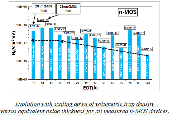
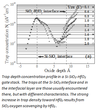
A few years ago, HfO2, a “high–k” dielectric, has been introduced in production to replace conventional SiO2 as gate insulator (Intel 2007). This allowed to obtain identical channel control with higher dielectric thickness and therefore to reduce gate leakage current (SiO2 thickness < 2 nm at that time). However, in addition to a thin SiO2 interfacial layer that grows during HfO2 deposition, this change impacted carrier mobility, noise level and threshold voltage stability so that a huge effort has been carried out to better characterize these stacks and their interfaces. Charge pumping can be used for that.
 
Contact : Daniel Bauza
Support and collaborations : FMNT, MEDEA + Project FOREMOST, NANOSIL Network of Excellence, collaboration LETI-CEA, ST Microelectronics.
See for instance : O. Ghobar et al. “Defects in the interfacial layer of SiO2-HfO2 gate stacks: depth distribution and identification,” IEEE International Reliability Workshop (IIRW), Stanford Sierra Conf. Center - S. Lake Tahoe, CA, USA, October 15-18, 2007. 

Date of update November 17, 2023

French
CROMA
Grenoble site
Grenoble INP - Minatec : 3, Parvis Louis Néel - CS 50257 - 38016 Grenoble Cedex 1

Chambery site
Université Savoie Mont Blanc - Rue Lac de la Thuile, Bat. 21 - 73370 Le Bourget du Lac
 
 
République Française         Logo CNRS_2019        Logo Grenoble INP - UGA   Grenoble Alps University    Université Savoie Mont Blanc
Université Grenoble Alpes