Aller au menu Aller au contenu
Thèmes de recherche
Microélectronique, électromagnétisme, photonique, hyperfréquences
Thèmes de recherche
Thèmes de recherche

> Recherche > CMNE > CMOS & technologies alternatives

CMOS ultime et technologies alternatives

Responsable : Gérard GHIBAUDO

Contexte et objectifs

L’axe « CMOS » de CROMA jouit d’une réputation internationale reconnue depuis plus de 30 ans en matière de conception et de caractérisation des dispositifs à semi-conducteurs. Il a été notamment pionnier dans l’étude et la promotion des technologies CMOS sur SOI. Notre mission générique consiste à explorer et étendre les frontières de la micro- et nano-électronique CMOS. L’objectif permanent du groupe est la compréhension des mécanismes physiques en vue de leur utilisation pour le développement des technologies, des dispositifs et de leurs applications.

Nos activités de recherche se déroulent notamment dans le contexte du Labex MINOS sur Minatec et en lien étroit avec nos partenaires locaux (CEA, ST, SOITEC, …) et internationaux (réseaux et projets européens, accords bilatéraux…). Elles sont par ailleurs largement soutenues par des projets européens et nationaux.

Nouveaux matériaux et nouvelles architectures MOS

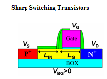
Convaincus que les variantes SOI assureront l’expansion future du CMOS et la transition de la micro- vers la nano-électronique, nous y consacrons beaucoup d’efforts sur deux plans : matériaux et dispositifs. Sur la base des technologies silicium, nous étudions les matériaux alternatifs au silicium massif (SOI, GeOI, Si contraint, SiC, III-V, GaN, etc.) ainsi que les nouvelles architectures de transistors MOS et de mémoires associées. L’accent est mis notamment sur les composants à faible pente sous le seuil pour les applications combinant performance et faible consommation.

Keywords: SOI, ultra-thin body and BOX (UTBB), GeOI, grilles multiples, nanofils(NW), MOSFET III-V, Tunnel FET, steep slope, floating body effects, ReRAM, NVM, variabilité spatiale et dynamique…

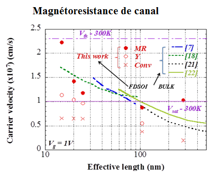
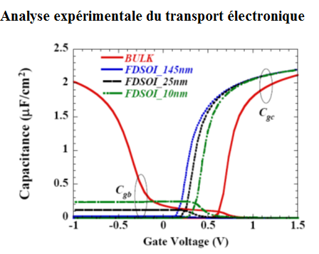
Caractérisation du transport et des interfaces diélectriques

Notre expertise dans ce domaine est fortement sollicitée pour évaluer le potentiel des matériaux alternatifs (pour le canal, la grille et les isolants enterrés), les effets de l'ingénierie de contrainte mécanique dans le canal et l’influence de l’architecture du transistor (films ultra-minces, grilles multiples, FinFET, JLT, nanofils, etc.). Notons que la pertinence d’une option technologique doit toujours être évaluée pour des canaux courts typiques du nœud technologique car les conclusions peuvent différer notablement de celles obtenues en canal long !

Keywords: mobilité des électrons et des trous, vitesse des électrons et des trous, vitesse de saturation, vitesse d’injection thermoïonique, transport hors d’équilibre, processus d’interaction, transport balistique, confinement et couplages quantiques, couplage entre canaux de conduction, inversion volumique, pièges d’interface, défauts…

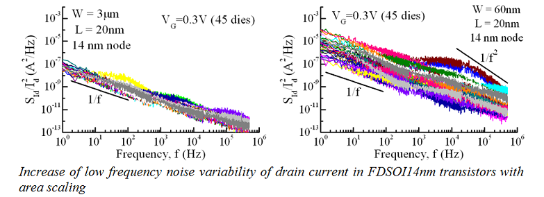
Techniques de caractérisation et des méthodologies d’extraction de paramètres

La compréhension de la physique de ces nouveaux composants passe par la capacité des expérimentateurs à extraire à partir des caractéristiques électriques des paramètres physiquement pertinents caractéristiques des différents phénomènes impliqués (couplage électrostatique, transport électronique, piégeage/dépiégeage des porteurs, effets quantiques, etc). Pour maintenir cette expertise au meilleur niveau mondial, nous développons en permanence nos techniques de caractérisation, les modèles physiques sous-jacents et nos outils de simulation.

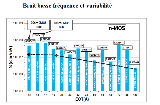
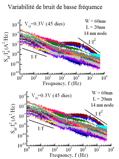
Keywords: pseudo-MOS, Y-function, split CV, analyse G-w, transitoires, effet Hall, magnétoresistance de canal, pompage de charge, bruit basse fréquence (LFN), mesures à basse température…

Filières alternatives au silicium

Les filières alternatives au silicium (SiC, GaN, substrats organiques, graphène) constituent également des sujets importants qui, de plus, démontrent notre volonté d’ouverture tout en utilisant à bon escient notre expertise en physique des dispositifs à semi-conducteurs.


Exemples

Robust fabrication of suspended ribbons made of CVD graphene with scalable fabrication techniques

Graphene devices 
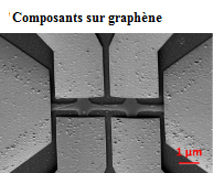
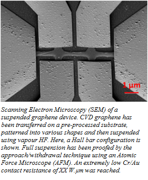
While it has been extensively proven that graphene was featuring many extraordinary properties that make it potentially interesting in a wide variety of fields, its full development will only be possible once scalable and robust fabrication routes compatible with large substrates will be available. This is a real challenge. Graphene growth by CVD on metal catalyst layer and its transfer to any type of substrate are first steps in this direction. However, processing such an ultra-thin layer of organic composition is not straightforward, with many issues to be solved, related for instance to capillary effects, control of ad-hesion, residual strain or incompatibility with some usual cleaning processes. We have succeeded in developing such a route for the fabrication of suspended structures. This opens the field to a variety of applica-tions, for instance in the field of NEMS.
Contact: Mireille MOUIS
Support and collaborations: CNRS network of technological facilities Renatech (clean rooms for device fabrication), Georg Düsberg’s team, Trinity College, Dublin (growth and transfer of CVD graphene)
See for instance: O. I. Aydin, T. Hallam, J.L. Thomassin, M. Mouis, and G. Duesberg, Challenges in Suspending CVD Graphene:More than Capillary Effects, 15th International Conference on Ultimate Integration on Silicon (ULIS), 8-9 April 2014, Stockholm, Sweden, IEEE, Proceedings of ULIS 2014, pp. 33-36, doi: 10.1109/ULIS.2014.6813899 (2014)

Channel magnetoresistance in the saturation regime of operation MOS transistors: a new insight into high field transport


Magnétoresistance de canal
It has been shown that channel magnetore-sistance, measured under transverse mag-netic field in the linear regime of operation (low VDS) of MOSFET transistors of wide and short geometry, could be used to ex-tract channel mobility (µMR) without being influenced by uncertainties on the exact value of channel length which is less pre-cisely known as device dimensions de-crease. We have recently shown that the B2 dependence of channel magnetoresistance is observed in the whole range of bias volt-ages, from linear regime to saturation (from low to high VDS). It can be used to extract an apparent mobility, which varies with gate and drain voltages. These variations are fully explained by a new physical compact model that we have developed, from which both linear mobility at low field and high field velocity can be extract-ed. When applied to 14nm FDSOI devices, this new method showed that high field operation was driven by out-of-equilibrium transport without being yet ballistic.
 
Contact : Gérard Ghibaudo, Mireille Mouis
Support and collaborations:  LCMI (high magnetic field), STMicroelectronics (devices pro-vision)
See for instance : Minju Shin, Ming Shi, Mireille Mouis, Antoine Cros, Emmanuel Josse, Ben-jamin Piot, Gyu-Tae Kim and Gérard Ghibaudo, Experimental and theoretical investigation of magnetoresistance from linear operation to saturation in 14nm FDSOI MOS devices, submit-ted to IEEE Transactions on Electron Devices, 2014
 
 ]
Simulation of gate capacitance variation
The split-CV method consists in analysing the gate to channel (CGC) and gate to sub-strate (CGB) capacitances variation with gate voltage (VG). It is a powerful method to extract physical information about elec-tron transport, charge control, or device physical characteristics (doping level, oxide thickness, etc.). However, when SOI substrates started to be used instead of bulk silicon, it became impossible to exploit CGB, due to buried oxide (BOX) thickness. We have shown that the emergence of ul-tra-thin BOX devices with backplane volt-age control could revive the method. By combining the full split CV technique with backplane voltage variation, we demon-strated that it was possible to extract physi-cal characteristics of the whole stack, from backplane to front gate. New parameters can be extracted while others are more directly evaluated and thus more reliable.

Contact : Gérard Ghibaudo, Mireille Mouis
Support and collaborations: CATRENE/Reaching22, ENIAC/Places2Be, in collaboration with STMicroelectronics (device provision)
See for instance :  Minju Shin, Ming Shi, Mireille Mouis, Antoine Cros, Emmanuel Josse, Gyu-Tae Kim and Gérard Ghibaudo, Full split C-V method for parameter extraction in Ultra Thin BOX FDSOI MOS devices, Solid-State Electronics, accepted 16 Apr. 2014, first published online 10 May 2014, doi: 10.1016/j.sse.2014.04.039 (May 2014).

Evolution of low frequency noise and noise variability through CMOS bulk technology nodes from 0.5 ?m down to 20 nm

We use low frequency noise (LFN) analysis as a non-destructive experimental tool to evaluate the quality of dielectric interfaces, which have a direct impact on electronic devices quality. Evaluating LFN behavior through several technology nodes can thus provide a global idea about device noise behavior and interface quality. Furthermore, CMOS scaling down is ac-companied by a reduction of device area, which subsequently leads to important issues related to statistical parameter variability. In this respect, LFN, which scales inversely with device area, is becoming a major concern not only for analog but also for digital circuits operation. In particular, LFN can limit the performance of VCO, DRAMs, SRAM cells, inverters and other mixed signal circuits. In addition, LFN is also subjected to variability due to device-to-device dispersion. This can also affect seriously integrated circuit functionality. For these reasons, it is required to study in detail LFN and its variability through CMOS technology nodes.
Evolution with scalling down of volumetric trap density
 
In this context, we carried out a thorough investigation of LFN and statistical noise variability through CMOS planar bulk technologies manufactured along the past 12 years and extended to the most recent 20 nm CMOS bulk technology node for the first time. The evolution with time and technology generation was studied by plotting oxide trap density Nt as a function of equivalent oxide thickness (EOT). It was found that Nt increased by almost two decades while EOT decreased from 12 nm (for the 0.5 ?m node) to 1.3 nm (for the 20 nm node) for n- and p-MOS. In spite of this trend, the LFN statistical variability has been surprisingly well controlled. It has even been improved for the 28 and 20 nm nodes.
Contact : Gérard Ghibaudo
Collaborations:  STMicroelectronics and CEA-LETI
See for instance : E. G. Ioannidis, S. Haendler, C. G. Theodorou, S. Lasserre,  C. A. Dimitriad-is, G. Ghibaudo, Evolution of low frequency noise and noise variability through CMOS bulk technology nodes from 0.5 ?m down to 20 nm, Solid State Electronics, 95, 28-31 (2014).

Low frequency noise variability

As device dimensions are scaling down, variability is increasing. This does not only concern dimensions, doping levels and static parameters but also dynamic parameters such as the low frequency noise (LFN). This has important implications as it can raise issues during device operation. The figure below shows how the statistical variability of LFN increases when device width decreases from 3µm to 60nm for the same technology (14nm node) and with the same number of dies included in the statistics (45 dies).
Increase of low frequency noise variability

Contact : Gérard Ghibaudo
Support and collaborations: STMicroelectronics. Projet ENIAC Places2Be
See for instance : E. G. Ioannidis, S. Haendler, C. G. Theodorou, S. Lasserre,  C. A. Dimitri-adis, G. Ghibaudo, Evolution of low frequency noise and noise variability through CMOS bulk technology nodes from 0.5 ?m down to 20 nm, Solid State Electronics, 95, 28-31 (2014).


Modeling basic charge pumping curves in various experimental conditions

Modeling basic charge pumping curves 
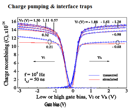
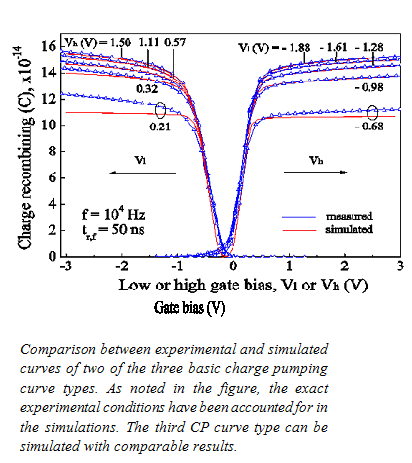
TheCharge pumping (CP) is a technique that applies on MOS transistors and allows the study of semiconductor-insulator interfaces traps. Depending on both, the specific CP technique used and the semiconductor-insulator studied, the mean interface trap density, the trap density vs. energy profile in the semiconductor bandgap, the traps capture cross-section or the trap density vs. insulator depth profile can be extracted. However, until recently, basic CP mecha-nisms were not correctly understood so that the three basic CP curve types had not been simulated satisfactorily. The figure shows two of these three basic curve types and their simulation. From the model that permitted these results, basic CP processes are validated along with the main Si-SiO2 interface traps properties introduced so that deeper studies of Si-SiO2 interface traps become possible.      
         
Contact : Daniel Bauza
Support: European network of Excellence NANOSIL, Catrene Project UTTERMOST. 
See for instance : D. Bauza, “On the meaning of charge pumping curve edges” International Reliability Physics Symposium (IRPS), April 14-18, 2013; Monterey, CA, USA, Proceedings pp. GD 2.1-2.4.; D. Bauza,“Charge pumping, an overview of the technique and recent new features,” Tutorial, 2011 IEEE International Integrated Reliability Workshop (IIRW) – Stanford Sierra Conf. Center - S. Lake Tahoe, CA, USA, October 16-20, 2011.      

The use of charge pumping for studying defects in high-k gate stacks.

Charge pumping and interface traps 
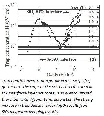
A few years ago, HfO2, a “high–k” dielectric, has been introduced in production to replace conventional SiO2 as gate insulator (Intel 2007). This allowed to obtain identical channel control with higher dielectric thickness and therefore to reduce gate leakage current (SiO2 thickness < 2 nm at that time). However, in addition to a thin SiO2 interfacial layer that grows during HfO2 deposition, this change impacted carrier mobility, noise level and threshold voltage stability so that a huge effort has been carried out to better characterize these stacks and their interfaces. Charge pumping can be used for that.
 
Contact : Daniel Bauza
Support and collaborations : FMNT, MEDEA + Project FOREMOST, NANOSIL Network of Excellence, collaboration LETI-CEA, ST Microelectronics.
See for instance : O. Ghobar et al. “Defects in the interfacial layer of SiO2-HfO2 gate stacks: depth distribution and identification,” IEEE International Reliability Workshop (IIRW), Stanford Sierra Conf. Center - S. Lake Tahoe, CA, USA, October 15-18, 2007. 

Sharp Switching Transistors

Circuit designers are dreaming about a device capable of very sharp switching between OFF and ON states, suitable for increasing the frequency of operation while reducing the power consumption. In collaboration with LETI-CEA, STMicroelectronics and Brown University (USA), we have developed several generations of tunnel transistors (TFET): from planar SOI to triple-gate hetero-nanowire SiGe/Si TFETs, which actually exhibit world record performance [1]. The core of our research is the characterization and modeling of physics mechanisms: band-to-band and trap assisted tunneling, temperature effects, low-frequency noise, ambipolarity, bi-layer tunneling.  

Two new devices with fascinating performance have been conceived and patented recently.

BET-FET – The Bipolar Enhanced TFET combines tunneling and bipolar transistors embedded within the same body. The revolutionary idea is to use the tunneling current as base current of the bipolar transistor. The collector current is an amplified (x1000) image of the tunneling current. Simulations predict that BETFETs can achieve very high ON-current (4 mA/µm) and sub-60 mV/decade subthreshold slope over 7 decades of current [2].

Z2-FET – The ‘Zero impaction ionization and Zero subthreshold swing field-effect transistor’ is a forward biased PIN diode with undoped body partially covered by the front gate (Fig. 1a) [3]. A negative gate bias VG and a positive substrate bias VBG generate two potential barriers which respectively block the electron injection from drain and the hole injection from source. The gate and substrate biases actually emulate by field effect a PNPN configuration without need for specific body doping. By increasing VG, the electron barrier is lowered enabling electrons to flow to the source where they cause the lowering of the hole barrier. This positive feedback instantaneously unblocks the device. Fig. 1b shows the transfer characteristics, where the current increases abruptly over 8 decades as VG is increased by 1mV only. This performance is unrivalled by classic MOS transistors. Further ID-VD measurements (Fig. 1c) reveal a VG-controlled hysteresis, which is useful for various applications: ESD protection of FDSOI circuits [4], capacitorless DRAM, single-transistor SRAM, sensing, fast logic, etc.

Sharp Switching Transistors
[1] A. Villalon et al, First demonstration of strained SiGe nanowires TFETs with ION beyond 700 µA/µm. 2014 Symposia on VLSI Technology and Circuits, Honolulu, USA, (9–13 june 2014).
[2] J. Wan, A. Zaslavsky, C. Le Royer, S. Cristoloveanu, Novel bipolar-enhanced tunneling FET with simulated high on-current. IEEE Electron Device Letts., 34, n? 1, 24–26 (2013).
[3] J. Wan, A. Zaslavsky, C. Le Royer, S. Cristoloveanu, A feedback silicon-on-insulator steep switching device with gate-controlled carrier injection. Solid-State Electronics, 76, 109–111 (2012).
[4] Y. Solaro et al, Innovative ESD protections for UTBB FD-SOI technology. IEDM'13, Washington DC, USA (9–11 dec. 2013).


Contact:
Sorin Cristoloveanu   Tél : +33 456 529 499.
 

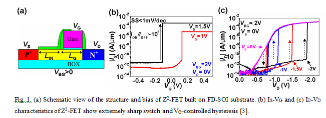
mise à jour le 10 janvier 2024

anglais
CROMA
Site de Grenoble
Grenoble INP - Minatec - 3, Parvis Louis Néel , CS 50257 - 38016 Grenoble Cedex 1

Site de Chambéry
Université Savoie Mont Blanc - Rue Lac de la Thuile, Bat. 21 - 73370 Le Bourget du Lac
 
 
République Française         Logo CNRS_2019       Logo Grenoble INP - UGA Université Grenoble Alpes      Université Savoie Mont Blanc
Université Grenoble Alpes