Aller au menu Aller au contenu
Centre for Radiofrequencies, Optic and Micro-nanoelectronics in the Alps

> News > Events-PhD_Defenses

PhD Defense of Jessy MICOUT

Published on March 1, 2019
A+Augmenter la taille du texteA-Réduire la taille du texteImprimer le documentEnvoyer cette page par mail cet article Facebook Twitter Linked In
PhD Defense March 8, 2019 | Access map
Defense of the doctoral thesis of MICOUT Jessy,  for the University Grenoble Alpes, speciality  " NANO ELECTRONICS & NANO TECHNOLOGIES ", entitled:
 
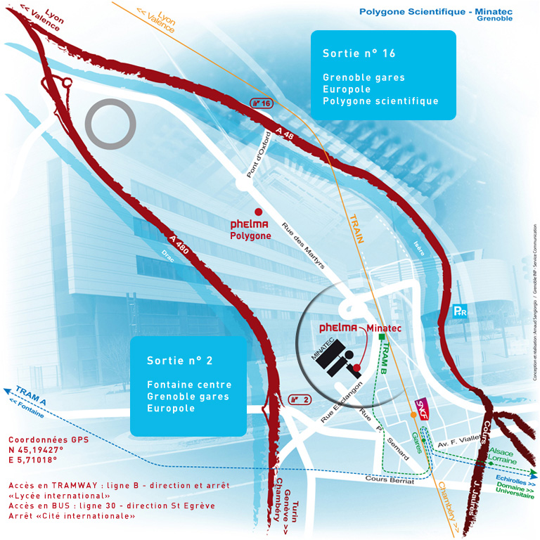
Room Z104- Building Phelma 2/MINATEC
3 rue parvis Louis Néel
38016 Grenoble cedex1

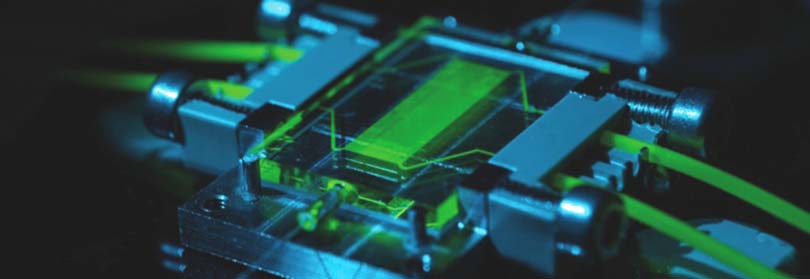
Fabrication and Characterisation of low temperature transistors

MICOUT Jessy

MICOUT Jessy

Friday, March 8, 2019  at 10:30


Abstract:
The down scaling of MOSFET device is becoming harder and the development of future generation of MOSFET technology is facing some strong difficulties. To overcome this issue, the vertical stacking of MOSFET in replacement of the conventional planar structure is currently investigated. This technique, called 3D VLSI integration, attracts a lot of attention, in research and in the industry. Indeed, this sequential stacking of transistor enables to gain in density and performance without reducing transistors dimensions.
More specifically, 3D sequential integration or CoolCube™ at CEA-Leti enables to fully benefit of the third dimension by sequentially manufacturing transistors. Implementing such an integration provides the new constraint of manufacturing top transistor with low thermal budget (below 500°C) in order to preserve bottom-transistor performances. As most of the thermal budget is due to the dopant activation, several innovative techniques are currently investigated at CEA-LETI.
In this work, solid phase epitaxy regrowth will be used as the mechanism to activate dopants below 600°C. The aim of this thesis is thus to manufacture and to characterize transistors with low-temperature dopant activation, in order to reach the same performance as devices manufactured with standard thermal budget. The work is organized around the dopant activation, and in three chapters, according to each considered integration scheme (Extension Last/ Extension First, Gate Last/ Gate First) and architecture (FDSOI, FINFET). These chapters, assisted by relevant simulations, electrical and morphological characterizations, will enable to develop a new and stable 500°C recrystallization process for both N and P FETs, and to propose new integration schemes in order to manufacture transistors with low thermal budget and compatible with the 3D sequential integration.
 
Members of jury :
  • Francis BALESTRA, Director  of research CNRS Alpes :President
  • Gérard GHIBAUDO,Director  of research CNRS Alpes : Supervisor
  • Professor Pascal MASSON, University Sophia Antipolis : Rapporteur
  • Fuccio CRISTIANO, Directeur de recherche CNRS Toulouse: Rapporteur
  • Doctore Perrine BATUDE, CEA Grenoble : Member
  • Doctor Quentin RAFHAY, Grenoble INP : Member

A+Augmenter la taille du texteA-Réduire la taille du texteImprimer le documentEnvoyer cette page par mail cet article Facebook Twitter Linked In

Partenaires

Thesis prepared in the laboratory IMEP-LaHC  and  CEA, supervised by Gérard GHIBAUDO .

Date of update March 21, 2019

French
CROMA
Grenoble site
Grenoble INP - Minatec : 3, Parvis Louis Néel - CS 50257 - 38016 Grenoble Cedex 1

Chambery site
Université Savoie Mont Blanc - Rue Lac de la Thuile, Bat. 21 - 73370 Le Bourget du Lac
 
 
République Française         Logo CNRS_2019        Logo Grenoble INP - UGA   Grenoble Alps University    Université Savoie Mont Blanc
Université Grenoble Alpes