Aller au menu Aller au contenu
Centre for Radiofrequencies, Optic and Micro-nanoelectronics in the Alps

> News > Events-PhD_Defenses

PhD Defense of Theano KARATSORI

Published on July 3, 2017
A+Augmenter la taille du texteA-Réduire la taille du texteImprimer le documentEnvoyer cette page par mail cet article Facebook Twitter Linked In
PhD Defense July 12, 2017 | Access map
Defense of a doctoral thesis of Theano KARATSORI, for the University Grenoble Alpes , speciality "NANO ELECTRONIC & NANO TECHNOLOGIES ", entitled:

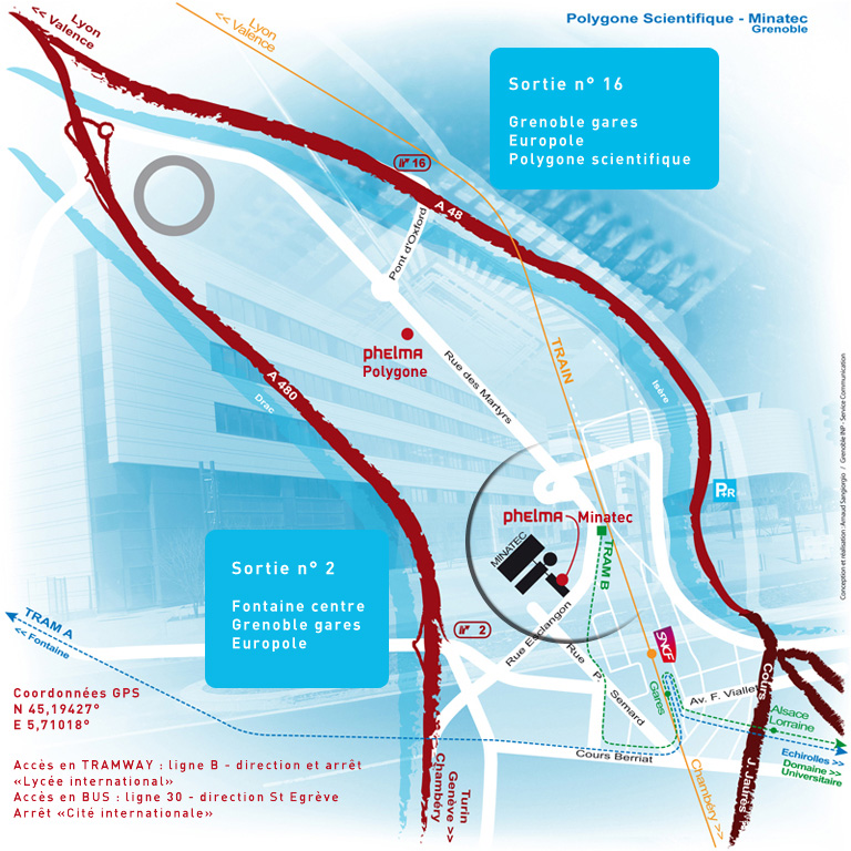
Amphi  Z-108 Phelma/Minatec
3 rue parvis Louis Néel
38016 Grenoble cedex1

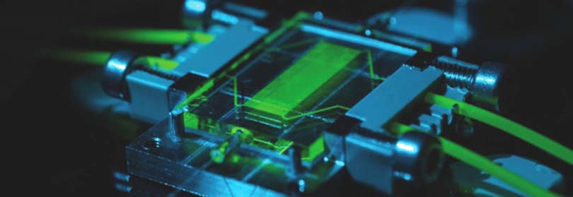
« Electrical Characterization and Modeling of Advanced Nano-scale Ultra Thin Body and Buried Oxide MOSFETs and Application in Circuit Simulations »

Theano KARATSORI

Theano KARATSORI

Wednesday, July 12nd, 2017 at  10:30

Abstract:
Τhe motivation for this dissertation is two of the main issues brought up by the scaling of new-era devices in contemporary MOSFET design: the development of an analytical and compact drain current model, valid in all regions of operation describing accurately the transfer and output characteristics of short-channel FDSOI devices and the investigation of reliability and variability issues of such advanced nanoscale transistors. Chapter II provides a theoretical and technical background for the better understanding of this dissertation, focusing on the critical MOSFET electrical parameters and the techniques for their extraction. It demonstrates the so-called Y-Function and Split-CV methodologies for electrical characterization in diverse types of semiconductors. The influence of AC signal oscillator level on effective mobility measurement by split C-V technique in MOSFETs is also analyzed. A new methodology based on the Lambert W function which allows the extraction of MOSFET parameters over the full gate voltage range, enabling to fully capture the transition between subthreshold and above threshold region, despite the reduction of supply voltage Vdd is presented. Finally, some basic elements concerning the low frequency noise (LFN) on MOSFETs characterization are described. Chapter III presents the analytical drain current compact modeling in nanoscale FDSOI MOSFETs.
Simple analytical models for the front and back gate threshold voltages and ideality factors have been derived in terms of the device geometry parameters and the applied bias voltages with back gate control. An analytical compact drain current model has been developed for lightly doped UTBB FDSOI MOSFETs with back gate control, accounting for small geometry and other significant in such technologies effects and implemented via Verilog-A code for simulation of circuits in Cadence Spectre. Chapter IV is dealing with reliability issues in FDSOI transistors. The hot-carrier degradation of nanoscale UTBB FDSOI nMOSFETs has been investigated under different drain and gate bias stress conditions. The degradation mechanisms have been identified by combined LFN measurements at room temperature in the frequency and time domains. Based on our analytical compact model of Chapter III, an HC aging model is proposed enabling to predict the device degradation stressed under different bias conditions, using a unique set of few model parameters determined for each technology through measurements. Finally, the NBTI stress characteristics and the recovery behavior under positive bias temperature stress of HfSiON gate dielectric UTBB FDSOI pMOSFETs have been investigated. A model for the NBTI has been developed by considering hole-trapping/detrapping mechanisms, capturing the temperature and bias voltage dependence. In Chapter V studies of variability issues in advanced nano-scale devices are presented. The main sources of drain and gate current local variability have been thoroughly studied. In this aspect, a fully functional drain current mismatch model, valid for any gate and drain bias condition has been developed. The main local and global variability MOSFET parameters have been extracted owing to this generalized analytical mismatch model. Furthermore, the impact of the source-drain series resistance mismatch on the drain current variability has been investigated for 28nm Bulk MOSFETs. A detailed statistical characterization of the drain current local and global variability in sub 15nm Si/SiGe Trigate nanowire pMOSFETs and 14nm Si bulk FinFETs has been conducted. Finally, a complete investigation of the gate and drain current mismatch in advanced FDSOI devices has been performed. Finally, the impact of drain current variability on circuits in Cadence Spectre is presented. An overall summary of this dissertation is presented in Chapter VI, which highlights the key research contributions and future research directions are suggested.

Members of jury :
- Gérard GHIBAUDO : Supervisor
- Charalabos DIMITRIADIS : Co-Supervisor
- Dimitrios TASSIS : Examiner
- Francis BALESTRA : Examiner
- Nathalie MALBERT : Reviewer
- Brice GAUTIER : 
Reviewer

A+Augmenter la taille du texteA-Réduire la taille du texteImprimer le documentEnvoyer cette page par mail cet article Facebook Twitter Linked In

Partenaires

Thesis prepared in the laboratory : UMR 5130 - IMEP-LAHC  (Institut de Microélectronique, Electromagnétisme, Photonique – Laboratoire Hyperfréquences et Caractérisation) supervised by Gérard GHIBAUDO and  Charalabos DIMITRIADIS - Co-supervisor (Aristotle University of Thessaloniki ).
 

Date of update July 4, 2017

French
CROMA
Grenoble site
Grenoble INP - Minatec : 3, Parvis Louis Néel - CS 50257 - 38016 Grenoble Cedex 1

Chambery site
Université Savoie Mont Blanc - Rue Lac de la Thuile, Bat. 21 - 73370 Le Bourget du Lac
 
 
République Française         Logo CNRS_2019        Logo Grenoble INP - UGA   Grenoble Alps University    Université Savoie Mont Blanc
Université Grenoble Alpes