Special seminar
Published on September 18, 2013
A+Augmenter la taille du texteA-Réduire la taille du texteImprimer le documentEnvoyer cette page par mail
TUESDAY, SEPTEMBER 24,2013 from 4 to 5pm
Open to others researchers in the lab
Institut de Microélectronique, Electromagnétisme et Photonique
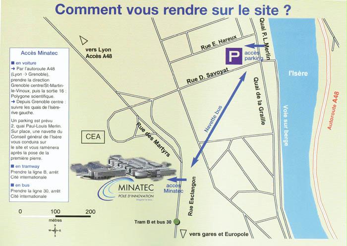
room BELLEDONNE , Minatec, Bât. Bcai
3 Parvis Louis Neel, CS 50257, 38016 GRENOBLE CEDEX 1, France
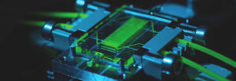
“Future of Nano CMOS Technology”
by Prof. Hiroshi IWAI (Tokyo Institute of Technology, Japan)
A+Augmenter la taille du texteA-Réduire la taille du texteImprimer le documentEnvoyer cette page par mail
Partenaires
TUESDAY , SEPTEMBER 24, 2013
Abstract:
Although silicon-based CMOS devices have dominated the integrated circuit applications over the past few decades, it is expected that the development of CMOS would reach its limits after the next decade because of the difficulties in downsizing and some fundamental limits of MOSFETs. However, there are no promising candidates which can replace CMOS with better performance with high-density integration for the moment. Thus, we have to stick to the CMOS devices until its end. In order to pursue the downsizing of CMOS for another decade, the development of new technologies is becoming extremely important. Not all the companies can necessarily develop the most advanced technology timely and the competition between the leading semiconductor manufacturing companies becomes very severe for their survive. The current status of the frontend of the technology is as follows: New device structures (FinFET, Tri-gate, and Si-nanowire MOSFETs) are replacing conventional planar MOSFETs. Continuous innovation of High-k/metal gate technologies has enabled EOT scaling down to 0.9 - 0.7 nm in production, however, new materials are necessary for further EOT scaling. Recent advances in new channel material such as III-V/Ge shows promising device performances, however, it is still behind of the state of the art Si-CMOS technologies. Device demonstration on emerging technologies (such as Tunnel FET, Junctionless FET, Carbon-based FET..) is increasing, but we cannot draw a successful story to replace the Si-CMOS and much longer time is needed for implementation of these technologies in future generation devices.Hiroshi Iwai received the B.E. and Ph.D. degrees in electrical engineering from the University of Tokyo and worked in the research and development of integrated circuit technology for more than 25 years in Toshiba. He is now a professor of Frontier Research Center and Dept. of Electronics and Applied Physics, Interdisciplinary Graduate School of Science and Engineering, Tokyo Institute of Technology, Yokohama, Japan. Since joining Toshiba, he has developed several generations of high density static RAM's, dynamic RAM's and logic LSI's including CMOS, bipolar, and Bi-CMOS devices. He has also been engaged in research on device physics, process technologies, and T-CAD related to small-geometry MOSFETs and high speed bipolar transistors. He has authored and coauthored more than 1,000 international and 400 domestic journal/conference papers. Dr. Iwai is a fellow of IEEE, a fellow of Institute of Electrical Engineers Japan, a fellow of the Japan Society Applied Physics, and a fellow of the Institute of Electronics, Information and Communication Engineers of Japan.
Date of update December 3, 2014
Our sites
eServices


")


