1 year post-doctoral position - 2016
Published on October 21, 2015
A+Augmenter la taille du texteA-Réduire la taille du texteImprimer le documentEnvoyer cette page par mail
from January 1, 2016 to January 1, 2017
|
Access map
Job period :
Position open from Janoary 1st 2016
12 months Postdoc position in the frame of HETONAN ANR project.
Subject:
Simulation and modelling of high efficiency tandem solar cells based on III-V nanowires on silicon
Context:In the present context of greater need for efficient renewable energies, the increase of cost effectiveness of photovoltaic (PV) electricity production is compulsory.
In this scope, the strategy for further cost reductions for PV installations mainly rely on better module efficiency in order to increase the power delivered per m². For mainstream photovoltaics based on crystalline Si, the efficiency, which lies today between 20% for high quality commercial modules and 25.6% for laboratory prototypes, cannot exceed the fundamental Shockley-Queisser limit of 30%. Thin film solar cells (CdTe, CIGS, a-Si and related coumpounds) have emerged during the past ten years as a main competitor thanks to a slightly lower cost of fabrication but with limited potential efficiency. In order to overcome this 25% limit, one enabling technology is based on multi-junction solar cells, coupling several materials and band-gaps to optimize the
absorption of the solar spectrum (Figure 1). Each subcell type converts a certain wavelength, in each range of the solar spectrum. They are electrically connected in series using tunnel junctions, as shown in fig. 1.
These cells are challenging to produce because the electrical characteristics of the individual junctions must be matched and grown on a Germanium (Ge) substrate. In particular, the photocurrents generated in each junction must be close to the current generated by the other junction. There is hence a limited set of materials able to fulfill these conditions, and the most suitable ones are certainly Ge and III-V semiconductors.
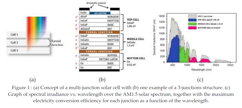
Due to the cost of Ge substrates or III-V materials, using this technology will not be possible for low cost application, but rather for terrestrial concentrated photovoltaics (CPV).
New alternative technological approaches are therefore required to combine high efficiency with cost reduction.
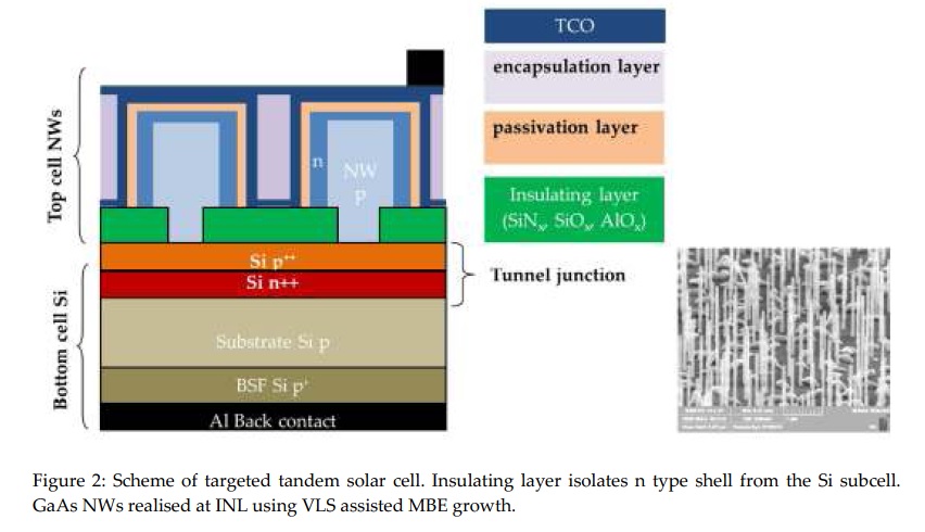
The aim of the HETONAN project is hence to combine the advantages of existing silicon technology with those of emerging III-V technology, in order to develop a high efficiency tandem cell for terrestrial applications.The main difficulty to achieve this goal lies in the complex direct growth of planar III-V films on Si substrate due to the strong lattice mismatches between Si and III-V materials.
To overcome this drawback, the HETONAN project aims to use a new concept, which consists in mixing III-V Nanowires (NWs) technology for the top cell (at 1.7 eV) with a standard Si bottom cell (at 1.12eV).The III-V NWs based top cell proposed here would then offer the significant advantage of being fabricated on a Si support, which is relatively cheap and processed with well-established techniques. Preliminary calculations have already confirmed that the cell efficiency potential for such tandem cell device would be 35 % higher compared to conventional single-junction silicon solar cells.
In this context, the precise estimation of the theoretical performance of such tandem cell is of paramount importance. Within the HETONAN project, a postdoc position is opened to work on the optoelectronic simulation of the proposed tandem solar cell. The aim of this work will be to define the optimal NW solar cell design and to simulate the tandem device performance by coupling optical and electrical modelling.
First, electromagnetic simulations will be carried out to define the best nanowire geometry for the absorption of light and to optimise current matching between the subcells. Simulations will be compared to experimental optical measurements of the samples fabricated in the framework of the HETONAN project.
Optical simulations will be then used as an input for electrical simulations in order to optimise the carrier collection efficiency and to estimate the power conversion efficiency of the solar cell. Optical simulations will be performed with an in-house Rigorous Coupled Wave Analysis software (RCWA) developed at IMEP-LAHC by Davide Bucci, which have already been used to optimize thin film nanowire based solar
cells [1,2]. Electrical simulation will be performed by TCAD commercial software (Sentaurus or Silvaco) [2].
Complementary to the simulation, electrical characterisations at low temperatures will be performed to analyse transport mechanisms in the structure and to adjust the simulations on the experimental results.
[1] A. Benali et al, Optical simulation of multijunction solar cells based on III-V nanowires on silicon, Energy Procedia
60 ( 2014 ) 109 – 115.
[2] J. Michallon et al., Toward an efficient extremely thin absorber solar cell based on ZnO nanowire arrays, 40th IEEE
Photovoltaic Specialist Conference (2014, Denver, USA).
A+Augmenter la taille du texteA-Réduire la taille du texteImprimer le documentEnvoyer cette page par mail
Date of update November 18, 2015
Our sites
eServices


 > Jobs

