Aller au menu Aller au contenu
Centre for Radiofrequencies, Optic and Micro-nanoelectronics in the Alps

> News > Events-PhD_Defenses

PhD Defense of Mehdi DAANOUNE

Published on January 22, 2015
A+Augmenter la taille du texteA-Réduire la taille du texteImprimer le documentEnvoyer cette page par mail cet article Facebook Twitter Linked In
February 3, 2015 | Access map
Defense of a doctoral thesis of Mehdi DAANOUNE  for the University of Grenoble, speciality Nano Electronics and NanoTechnlologies (NEET) entitled:
Amphitheater M001-Grenoble INP - Phelma
3 Parvis Louis Néel - CS 50257
38016 Grenoble Cedex 01

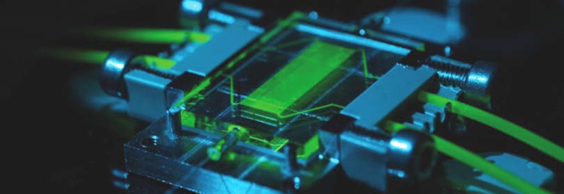
" Measurement of the lifetime and diffusion length of minority charge carriers in low dimensionality materials "

DAANOUNE Mehdi

DAANOUNE Mehdi

Tuesday, Febroary 3, 2015 at  10:30

Abstract:
The minority carrier lifetime is one of the main parameters used to analyse the semiconductors quality and photoconductivity decay (PCD) is one of the most widely used lifetime characterization method. Thanks to the variety of automated equipment that has developed, lifetime measurement has become a routine technique to assess the quality of semiconductors. However, the micro and nano materials used in the photovoltaic and microelectronics industry require an adaptation of the existing methods (PCD, photoluminescence etc.). Indeed, with reduced dimensions (epitaxial layers, SOI “Silicon on Insulator”, nanostructures and nanowires), the influence of the surface (interface states density, traps, etc.) becomes predominant. The presence of the substrates used for the material growth or for the layer transfer can also influence the measures. Consequently traditional methods of lifetime measurement are difficult to apply to low dimensional materials. This thesis is focused on the measurement of minority carrier lifetime in micro and nano materials (bulk, epitaxial layer, silicon on insulator and nanowires) with a special emphasis on the adaptation of the characterization tools to the material thickness.
We have studied first bulk samples and epitaxial layers (with thicknesses around 50µm) by photoluminescence. We have developed a method to determine simultaneously the bulk lifetime and the surface recombination velocity using room temperature photoluminescence measurement. The procedure consists in measuring the photoluminescence intensity ratio at different incident laser wavelengths and power. These photoluminescence ratios are then compared with analytical simulations, which allow us to evaluate the surface recombination velocity and the bulk lifetime.
We have then investigated SOI (Silicon on insulator) structures with ultrathin semiconductor layers of the order of 100 nanometers. After a brief description of the manufacturing methods and of some of their uses, we have analyzed the existing electrical methods used to evaluate the quality of SOI substrates. This led us to propose a new characterization method to overcome the limitations of these techniques. This method is based on a current-voltage measurement in the dark and under illumination called PSEUDO-MOSFET (the substrate of the SOI structure serves as the transistor gate and the two contact points deposited on the silicon film are used as the source and drain). We applied this new method to characterize the lifetime of a SOI substrate and with the help of numerical simulation, we were able to explain the recombination mechanism associated with interfaces and extract the parameters.
Finally, the last chapter concerns the study of nanowires for photovoltaic applications. In the nanowires, the surface to volume ratio greatly increases leading to a decrease of the effective lifetime due to the increased influence of the surfaces. In this chapter, we have studied the minority carrier lifetime in core-shell nanowire-based solar cells under dark conditions with a purely electrical approach called reverse recovery transient (RRT). This method is based on storage time measurement which depends essentially on the amount of stored charges in the biased junction and can be used to calculate the minority carrier lifetime. Numerical simulations have also been done to explain the measurements and to validate the theory and the hypotheses used for parameter extraction.

Members of  jury :
Anne KAMINSKI-CACHOPO - Supervisor
Danièle BLANC-PELISSIER - Co-supervisor
Jean-Paul KLEIDER - Rapporteur
Olivier PALAIS - Rapporteur
Oleksiy NICHIPORUK - Examiner
Jean-Emmanuel BROQUIN – Examiner


A+Augmenter la taille du texteA-Réduire la taille du texteImprimer le documentEnvoyer cette page par mail cet article Facebook Twitter Linked In

Partenaires

Thesis prepared in the laboratory  IMEP-LaHC and INL  supervised by Anne KAMINSKI-CACHOPO, supervisor and   Danièle blanc-pelissier Co-supervisor.

Date of update February 1, 2016

Contact

Anne KAMINSKI-CACHOPO
Send a mail
French
CROMA
Grenoble site
Grenoble INP - Minatec : 3, Parvis Louis Néel - CS 50257 - 38016 Grenoble Cedex 1

Chambery site
Université Savoie Mont Blanc - Rue Lac de la Thuile, Bat. 21 - 73370 Le Bourget du Lac
 
 
République Française         Logo CNRS_2019        Logo Grenoble INP - UGA   Grenoble Alps University    Université Savoie Mont Blanc
Université Grenoble Alpes