Special seminar by Souvik MAHAPATRA - Tuesday, June 16, 2015
Published on June 8, 2015
A+Augmenter la taille du texteA-Réduire la taille du texteImprimer le documentEnvoyer cette page par mail
Open to all : teachers, students, researchers, administrative, technicians
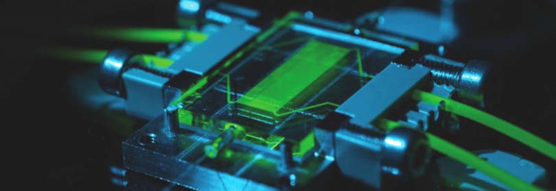
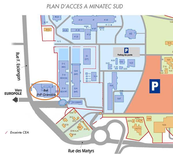
Room Belledonne, IMEP-LaHC, MINATEC
" Macroscopic and stochastic aspects of negative bias temperature instability in CMOS devices and circuits "
Tuesday, June 16, 2015 from 11:00 to 12:00
Abstract:
Negative Bias Temperature Instability (NBTI) is a crucial reliability concern for modern day state-of-the-art CMOS technologies. NBTI results in shift in MOSFET parameters, such as threshold voltage, drain current, etc., over time, and therefore causes long-time failure of CMOS integrated circuits. It is very important to understand the fundamental physical mechanism responsible for NBTI and develop suitable models to predict device and resultant circuit degradation at end product life. In this talk, the underlying physical processes responsible for NBTI in High-K Metal Gate (HKMG) MOSFETs will be briefly reviewed. Defect generation in MOSFET gate oxide will be explained from both macroscopic and stochastic viewpoints, which will be respectively useful to explain NBTI degradation in large and small area devices. This novel simulation framework can explain DC and AC NBTI degradation under various operating conditions such as different operating voltage, temperature, frequency and duty cycle in large area devices, as well as NBTI variability in small area devices. Furthermore, a compact model will be developed to simulate NBTI induced circuit degradation using SPICE simulation, and specific example of variable NBTI impact on SRAM performance parameters, such as read and hold static noise margin and write access time will be discussed.
Souvik Mahapatra received his PhD in Electrical Engineering from IIT Bombay, Mumbai, India in 1999. During 2000-01, he was with Bell Labs, Lucent Technologies, Murray Hill, NJ, USA. Since 2002 he is with the Department of Electrical Engineering at IIT Bombay and currently holds the position of full professor. His current research interests are in the area of CMOS logic gate stacks - scaling and reliability. He has published more than 150 papers in peer reviewed journals and conferences, delivered invited talks and tutorials in major international conferences including at the IEEE IEDM and IEEE IRPS, and served as a committee member and session chair in several IEEE conferences. He is a fellow of the Indian National Academy of Engineering, senior member of IEEE and a distinguished lecturer of IEEE EDS.
A+Augmenter la taille du texteA-Réduire la taille du texteImprimer le documentEnvoyer cette page par mail
Partenaires
by Souvik Mahapatra
Dept. of Electrical Engineering, Indian Institute of Technology, Bombay, India
Date of update June 8, 2015
Our sites
eServices


