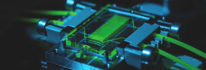
Heterogeneous 3D Chiplet Integration
Published on May 11, 2023
A+Augmenter la taille du texteA-Réduire la taille du texteImprimer le documentEnvoyer cette page par mail
Seminar
May 15, 2023
BELLEDONNE rrom & VIDEOCONFERENCE
Mitsumasa Koyanagi,
Prof. & GINTI Director/Senior Research Fellow à Tohoku University
")
Mitsumasa Koyanagi
Monday, May 15, 2023 at 10am
Abstract :
After introducing the research activities of 3D integration technologies in Tohoku University/GINTI, novel 3D chiplet integration technologies using self-assembly to achieve high-throughput and high-precision multichip-to-wafer stacking will be discussed. Many known good dies (KGDs) are simultaneously self-assembled on a carrier wafer with a high alignment accuracy making use of liquid surface tension. The self-assembled dies on the carrier are simultaneously transferred to another wafer or interposer wafer by de-bonding the carrier wafer after Cu nano-pillar hybrid bonding of self-assembled dies. In heterogeneous 3D integration, integration of MEMS, Si photonic chip and biochip onto CMOS chip will be discussed. In addition to achieve the future high density TSV and metal pad, we propose a new TSV formation methodology based on advanced Directed Self-Assembly (DSA) with nanocomposites consisting of nano metal particles and block-co-polymers and chip-to-wafer bonding technology to electrically connect small metal pads with a pitch of less than 0.5um using i-ACF film. Cylindrical nano-ordered structures with metal which act as nano-TSV are formed in Si deep holes through phase separation of polystyrene-block-poly methyl methacrylate polymers (PS-b-PMMA) are formed in TSV formation using DSA. An i-ACF film with high density Cu nano pillars with the diameter 60nm is inserted between the upper die and the lower die in chip-to-wafer bonding using i-ACF film.
I also explain our 3D AI chip fabricated using the heterogeneous 3D chiplet integration technology and implemented the vision transformer and the reservoir neural network algorithms on this 3D AI chip to perform the image recognition and voice recognition. I also briefly comment on post 5G technology and quantum computing based on heterogeneous 3D chiplet integration.
Mitsumasa Koyanagi was born in Hokkaido, Japan on 1947. He received the Ph.D. degree in electronic engineering from Tohoku University in 1974 and then joined Hitachi Ltd. where he worked on research and development of MOS memory device and process technology and invented a stacked capacitor DRAM memory cell which has been widely used in the DRAM production. In 1985, he joined the Xerox Palo Alto Research Center where he worked on research and developmen t of sub-micron CMOS devices and the design of analog/digital LSIs. In 1988 he joined Hiroshima University where he worked on sub-0.1um MOS devices, 3D integration technology, optical interconnection. Since 1994, he has been a professor in Tohoku University where his interests were 3D integration technology, optical interconnection, nano-CMOS devices, memory devices, parallel computer system, artificial retina chip and retinal prosthesis chip, brain-machine interface (BMI) and neural prosthesis chip. He established a small production line for 3D integration using 12-inch wafers called GINTI (Global Integration Initiative) in 2013 and became a director. Currently he is a senior research fellow in New Industry Creation Hatchery Center (NICHe), Tohoku University.
He has published more than 400 technical papers and given more than 200 invited talks. He was awarded IEEE Jun-ichi Nishizawa Medal, IEEE Cledo Brunetti Award, IEEE EPS Award, the National Medal Order of the Sacred Treasure, the National Medal with Purple Ribbon, the Award of Ministry of Education, Culture, Sports, Science and Technology in Japan and so on. He is an IEEE life fellow and a JSAP fellow.
A+Augmenter la taille du texteA-Réduire la taille du texteImprimer le documentEnvoyer cette page par mail
Date of update May 15, 2023
Our sites
eServices