Aller au menu Aller au contenu
Microelectronics, electromagnetism, photonics , microwave

> News > Events-PhD_Defenses

PhD Defense of Khadim DIENG

Published on November 16, 2016
A+Augmenter la taille du texteA-Réduire la taille du texteImprimer le documentEnvoyer cette page par mail cet article Facebook Twitter Linked In
PhD Defense November 23, 2016 | Access map
Defense of a doctoral thesis of Khadim DIENG for the University of  Grenoble Alpes , speciality  "NANO ELECTRONICS and NANO TECHNOLOGIES ", entitled:

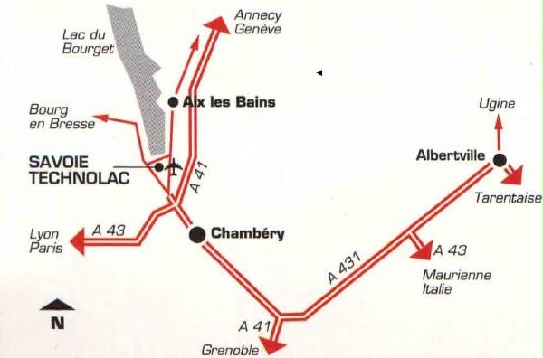
 Amphi Pôle Montagne- University Savoie Mont-Blanc
Campus scientifique du Bourget-du-Lac
73370-Le Bourget-du-Lac

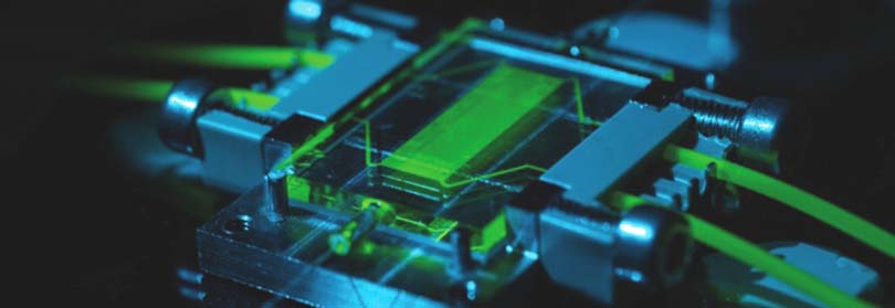
«Characterization and modeling of new capacitors "Through Silicon Capacitors" highly integrated to reducing consumption and to allow high frequency operating in 3D integrated circuit.»

Khadim DIENG

Khadim DIENG

Wednesday, November 23th, 2016 at 10:15

Abstract:
The decrease of transistor’s gate length was the key driver of the development of microelectronic integrated circuits in recent decades. However, this development of microelectronic circuits has led to a greater density of interconnection lines, generating high losses, slowdowns and crosstalk on the transmitted signals, and an increase of the parasitic impedance of interconnections lines. The latter is detrimental to the power integrity of the active components in the circuit. Its increase increases the risk of developing numerical errors leading to a system’s malfunction. It is therefore necessary to reduce the impedance of the power distribution network of integrated circuits. To do this, the decoupling capacitors are used and placed hierarchically on different floors of the circuits and in their entirety (PCB, package, interposer, chip).
These doctoral works are in the context of recent developments in new 3D integration solutions in microelectronics and they carry on studying new 3D capacitors, highly integrated, presenting high capacitance values (> 1 nF), and developed by using the depth of silicon interposeur level. Inspired from the Through Silicon Vias (TSV), these newly developed 3D capacitors are named Through Silicon Capacitors (TSC). They are a key element for improving the performance of the power integrated circuits because they can efficiently reduce the consumption of circuits thanks to their direct integration in silicon interposer which is used to stack chips. These 3D components allow tor reach high capacitance density up to 35 nF/mm². The issues are strategic for high speed embedded applications and more generally in an economic and societal environment aware of our energy limits. Moreover these decoupling capacitors must operate at frequencies up to 2 GHz or 4 GHz, which tend to maximize the parasitic effects which affect the energy efficiency of power distribution networks. This is made possible by optimizing their integration and by the use of copper layers with a good conductivity higher than 45 MS / m conductivity as electrodes.
The technologies used to fabricate the TSC are developed by CEA-LETI and STMicroelectronics. The electrical behavior of those TSC remained hitherto little known and their performances difficult to quantify. The studies conducted in this thesis were to model these new components by taking into account the material and geometrical parameters in order to know the parasitic effects. The established electrical models have faced electrical characterizations carried out over a wide frequency range (DC to 40 GHz). This work allow to optimize the TSC architecture and their integration in a power distribution network (Power Distribution Network - NDS) prove that they are good candidate for decoupling operations.
Keywords : Through Silicon Capacitors (TSC), 3D integration, Power distribution Networks (PDN), Energy efficiency, modeling and Characterization, Wide band frequency.
 
Members of jury :
  • Bernard FLECHET Supervisor
  • Bruno SAUVIAC Examiner
  • Francis CALMON Reviewer
  • Cédric BERMOND Co-Supervisor
  • Thierry LE GOUGUEC Reviewer

A+Augmenter la taille du texteA-Réduire la taille du texteImprimer le documentEnvoyer cette page par mail cet article Facebook Twitter Linked In

Partenaires

Thesis prepared in the laboratory : UMR 5130 - IMEP-LAHC  (Institut de Microélectronique, Electromagnétisme, Photonique – Laboratoire Hyperfréquences et Caractérisation) supervised by M.Bernard FLECHET , Supervisor .


Date of update November 16, 2016

French
CROMA
Grenoble site
Grenoble INP - Minatec : 3, Parvis Louis Néel - CS 50257 - 38016 Grenoble Cedex 1

Chambery site
Université Savoie Mont Blanc - Rue Lac de la Thuile, Bat. 21 - 73370 Le Bourget du Lac
 
 
République Française         Logo CNRS_2019        Logo Grenoble INP - UGA   Grenoble Alps University    Université Savoie Mont Blanc
Université Grenoble Alpes