Aller au menu Aller au contenu
Centre for Radiofrequencies, Optic and Micro-nanoelectronics in the Alps

> News > Events-PhD_Defenses

PhD Defense of Pierre TISSIER

Published on September 30, 2021
A+Augmenter la taille du texteA-Réduire la taille du texteImprimer le documentEnvoyer cette page par mail cet article Facebook Twitter Linked In
PhD Defense October 6, 2021 | Access map
Defense of doctoral thesis of Pierre TISSIER  for the  University  Grenoble Alpes, speciality  " NANO ELECTRONIQUE ET NANO TECHNOLOGIES ", entitled :
 
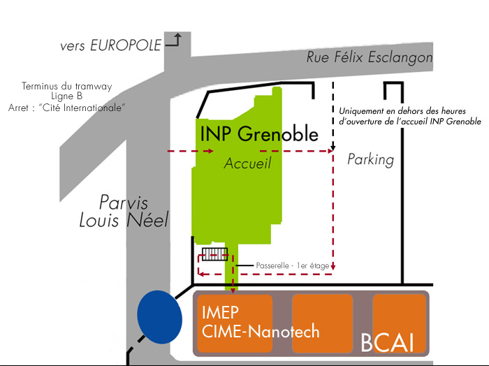
Room BELLEDONNE (Limited places)
IMEP-LaHC  - Minatec - 3, Parvis Louis Néel , CS 50257 -
38016 Grenoble Cedex
 

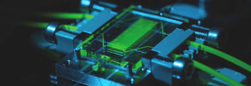
Opportunities and challenges of 3D integration for new photonic module architectures on Tbps/cm2 silicon

Pierre TISSIER

Pierre TISSIER

Wednesday, October 6, 2021 at 2:30 pm
 
Keywords:
3D Stacking,Photonic,TSV

Abstarct :
More and more data are produced and transmitted every year. The rise of new technologies such as high-performance computing or artificial intelligence require high bandwidth links between the different compute nodes and storage. Optical links, more performant and more power efficient than electrical links, are an interesting solution to address these needs. To interface the optical links and electronic compute elements, and to bring the optical link as close as possible to the compute element, a tridimensional architecture based on a photonic interposer is presented. This interposer is made from silicon so as to be compatible with the hosted compute chips, but also with the optical links with integrated silicon photonics elements. The cointegration of silicon photonics with 3D interconnexions needed for the photonic interposer is therefore mandatory to ensure adequate performance. This cointegration exhibits challenges, both on a microscopic and a macroscopic point of view. On a microscopic point of view, the presence of metallic interconnections can modify the optical properties of photonic devices nearby. This study aims to evaluate this perturbation, and to present optimal design rules to ensure correct optical performance. Experimental characterizations have shown that a minimal exclusion zone is required, even on the most sensitive optical elements. Complementary studies have been designed in order to study with accuracy the photo-elastic effect. This knowledge can be applied in the future for other domains where this effect also needs to be considered. On a macroscopic point of view, the interposer is prone to significant thermomechanical warpage which impeded final assembly. We measured quantitatively the chip warpage thanks to confocal optical profilometry at different temperature points. A compensation layer has also been designed and can be used to reduce the interposer warpage to values compatible with the chip dimensions. This compensation layer, fully compatible with the rest of the interposer process flow, has a variable material density, which enables it to be adapted to any considered architecture. Finally, technologies used in 3D interconnections have been applied to photonics, in particular to create thermal insulation cavities. These cavities thermally insulate optical components that require heat and reduce the global power consumption of the photonic interposer by reducing thermal losses. The challenges identified for the realization of the silicon photonic interposer have been addressed, and design rules have been established for the future architectures based on a silicon photonic interposer.

Jury members :
  • Jean-Emmanuel BROQUIN, Professor of Universities,University of Grenoble Alpes : Supervisor
  • Anne KAMINSKI-CACHOPO, Professor of Universities, Grenoble-INP : Examiner
  • Delphine MARRIS-MORINI, Professor of Universities, University Paris 11 - Paris SUD : Reviewer
  •  Ian O'CONNOR , Professor, Ecole Centrale Lyon : Reviewer
  •  François ROYER , Professor of Universities, University of Saint-Etienne - Jean Monnet : Examiner

A+Augmenter la taille du texteA-Réduire la taille du texteImprimer le documentEnvoyer cette page par mail cet article Facebook Twitter Linked In

Partenaires

Thesis prepared at  ST/ IMEP-LAHC (Institut de Microélectronique, Electromagnétisme & Photonique - Laboratoire d'Hyperfréquences et de Caractérisation) supervised by Jean-Emmanuel BROQUIN..

Date of update September 30, 2021

Contact

Jean-Emmanuel BROQUIN
Send a mail
French
CROMA
Grenoble site
Grenoble INP - Minatec : 3, Parvis Louis Néel - CS 50257 - 38016 Grenoble Cedex 1

Chambery site
Université Savoie Mont Blanc - Rue Lac de la Thuile, Bat. 21 - 73370 Le Bourget du Lac
 
 
République Française         Logo CNRS_2019        Logo Grenoble INP - UGA   Grenoble Alps University    Université Savoie Mont Blanc
Université Grenoble Alpes