Our sites
eServices
- Grenoble-Savoie Directory
- Maps & Directions
- CROMA Grenoble
- CROMA Chambéry

Our siteseServices

 > Research > CMNE > Modeling and Simulation

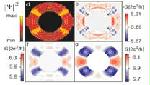

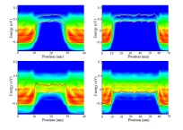
Examples of local density of states (LDOS) of silicon nanowire FETs with surface roughness and electron-phonon scattering as a function of the energy and of the position along the transport direction. |
This activity aims at developing numerical codes for the self-consistent simulation of nanoscale electron devices like nanowire or thin-body double-gate MOSFETs. Such codes solve the 3D or 2D equation of Schrödinger-Poisson with open boundary conditions along the transport direction. They are also able to treat the influence of spin-orbit coupling or of an external magnetic field. |
Contact: Marco Pala
Support: Agence National de la Recherche, « NOODLES » Project, « MOSINAS » Project, « QUASANOVA » Project, « QUANTAMONDE » Project.
EU commission, « COMPOSE3 » Project, « SQUWIRE » Project, « NANOSIL » NoE, « SINANO » NoE.
Relevant publications:
· S. Brocard, M.G. Pala and D. Esseni, Large On-Current Enhancement in Hetero-Junction Tunnel-FETs via Molar Fraction Grading, IEEE-Electron Device Letters 35, 184 (2014).
· M.G. Pala and D. Esseni, Interface Traps in InAs Nanowire Tunnel-FETs and MOSFETs—Part I: Model Description and Single Trap Analysis in Tunnel-FETs, IEEE Trans. Electron Devices 60, 2795 (2013).
· F. Conzatti, M.G. Pala, D. Esseni, Surface Roughness Induced Variability in Nanowire InAs Tunnel-FETs, IEEE-Electron Device Letters 33, 806 (2012).
· F. Conzatti, M.G. Pala, D. Esseni, E. Bano, and L. Selmi, Strain-induced performance improvements in InAs nanowire tunnel Fets, IEEE Trans. Electron Devices 59, 2085 (2012).
· A. Cresti, M.G. Pala, S. Poli, M. Mouis, and G. Ghibaudo, A Comparative Study of Surface-Roughness-Induced Variability in Silicon Nanowire and Double-Gate FETs, IEEE Trans. Electron Devices 58, 2274 (2011).
· S. Poli and M.G. Pala, Channel-Length Dependence of Low-Field Mobility in Silicon-Nanowire FETs, IEEE Electron Device Letters 30, 1515 (2009).
· S. Poli, M.G. Pala, T. Poiroux, S. Deleonibus, and G. Baccarani, Size dependence of surface-roughness-limited mobility in Silicon-nanowire FETs, IEEE Trans. Electron Devices 55, 2968 (2008).
· Th. Schäpers, V. A. Guzenko, M.G. Pala, et al., Suppression of weak antilocalization in GaInAs/InP narrow quantum wires, Physical Review B 74, 081301 (2006).
|
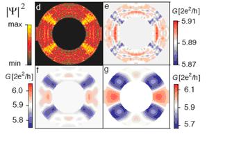
The observation of high quality integer quantum Hall effect in graphene at room temperature has galvanized the scientific community for the possible metrological applications (new standard of resistance) as well as for more fundamental physics aspects (as the degeneracy lifting of the graphene-specific zero Landau level). We investigate the interplay between magnetic field and disorder in determining the electronic transport properties of graphene ribbons. The combination of atomistic tight-binding description and full quantum Green’s function approach allows us to consider different types of experimentally relevant disorder sources as short-range potential (adsorbates, vacancies…), long-range disorder (charged impurities) and geometrical distortion (scrolls, ripples…). Depending on the disorder nature, interesting effects can be predicted, as for example the quenching of the integer quantum Hall effect in ribbons with scrolled edges or in narrow ribbons with moderate disorder. |
Contact: Alessandro Cresti
Recent publications:
· A. Cresti, M.M. Fogler, F. Guinea, A.H. Castro Neto and S. Roche, Quenching of the Quantum Hall Effect in Graphene with Scrolled Edges, Physical Review Letters 108, 166602 (2012).
· K.L. Chiu, M.R. Connolly, A. Cresti, C. Chua, S.J. Chorley, F. Sfigakis, S. Milana, A.C. Ferrari, J.P. Griffiths, G.A.C. Jones and C.G. Smith, Single-particle probing of edge-state formation in a graphene nanoribbon, Physical Review B 85, 205452 (2012).
· R. Ribeiro, J.-M. Poumirol, A. Cresti, W. Escoffier, M. Goiran, J.-M. Broto, S. Roche and B. Raquet, Unveiling the Magnetic Structure of Graphene Nanoribbons, Physical Review Letters 107, 86601 (2011).
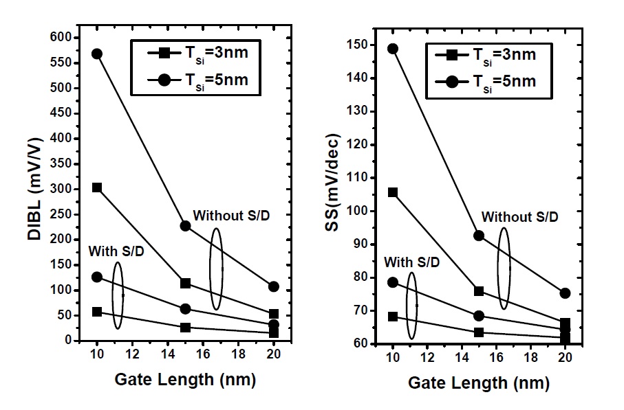 Analytical modeling of short channel effects showing the significant role of the source and drain on the value of DIBI and subthreshold slope (T. Dutta et al., ULIS Conference 2013 |
We are developing analytical models in order to capture as many effects as possible (e.g. quasi ballistic transport, source-drain leakage, accurate short channel effects etc.), that are playing a key role in nano MOSFETs. These models are extensively compared to advanced simulations codes (NEGF, TCAD, MC with our collaboration with DIEGM/Udine). In particular, many studies have been focused on the evaluation of Ge and III-V channel devices, which are presently a realistic option for the end of the roadmap. A strong collaboration with the Advanced Device group in ST Microelectrics allows us to transfert our model in the MaSTar plateform and hence reach a larger audience. |
Contact: Quentin Rafhay
Support: STREP Compose3 - ANR MOSINAS - ANR Noddle
See for instance: Quentin Rafhay, Raphaël Clerc, Gérard Ghibaudo, Georges Pananakakis, Impact of source-to-drain tunnelling on the scalability of arbitrary oriented alternative channel material nMOSFETs, Solid-State Electronics 52, 1474-1481 (2008).
Recent publications:
• B. Sklenard, P. Batude, Q. Rafhay, et al., Influence of device architecture on junction leakage in low-temperature process FDSOI MOSFETs, Solid-State Electronics 88, 9 (2013).
• T. Dutta, Q. Rafhay, et al., Impact of quantum effects on the short channel effects of III-V nMOSFETs in weak and strong inversion regimes, Solid-State Electronics 88, 43 (2013).
• I. Ben Akkez, A. Cros, C. Fenouillet-Beranger, F. Boeuf, Q. Rafhay, F. Balestra, G. Ghibaudo, New parameter extraction method based on split C–V measurements in FDSOI MOSFETs, Solid-State Electronics 84, 142 (2012).
• A. Zaka, P. Palestri, Q. Rafhay, R. Clerc, M. Iellina, D. Rideau, C. Tavernier, G. Pananakakis, H. Jaouen, L. Selmi, An Efficient Nonlocal Hot Electron Model Accounting for Electron-Electron Scattering, IEEE Trans. Electron Devices 59, 983 (2012).
• A. Zaka, J. Singer, E. Dornel, D. Garetto, D. Rideau, Q. Rafhay, R. Clerc, J.-P. Manceau, N. Degors, C. Boccaccio, C. Tavernier, H. Jaouen, Characterization and 3D TCAD simulation of NOR-type flash non-volatile memories with emphasis on corner effects, Solid-State Electronics 63, 158 (2012).
• A. Zaka, Q. Rafhay, M. Iellina, P. Palestri, R. Clerc, D. Rideau, D. Garetto, E. Dornel, J. Singer, C. Tavernier, G. Pananakakis, H. Jaouen, On the Accuracy of Current TCAD Hot Carrier Injection Models in Nanoscale Devices, Solid-State Electronics 54, 1669 (2010).
• M.F. Beug, Q. Rafhay, M.J. van Duuren, R. Duane, Investigation of Back-Bias Capacitance Coupling Coefficient Measurement Methodology for Floating-Gate Nonvolatile Memory Cells, IEEE Trans. Electron Devices 57, 1253 (2010).
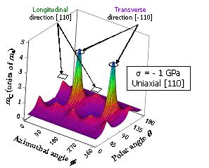
Calculation of the hole conduction mass reduction
due to a longitudinal compressive stress along the
[110] direction. In contrast, the transverse mass
almost keeps its unstrained value.
An analytical model of electron and hole mobility in strained silicon is being developed in order to describe low field transport along any channel orientation with an arbitrary stress configuration (arbitrary stress tensor). The model, which runs in a few seconds on a standard PC, is based on an exact solution of the 6x6 k.p Hamiltonian coupled with a Kubo-Greenwood approach for mobility calculation. It can be used to support the interpretation of experimental results in terms of strain induced mobility variations or to find channel orientations and stress configurations that optimize carrier transport.
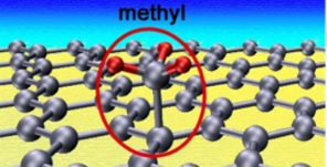
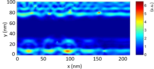
 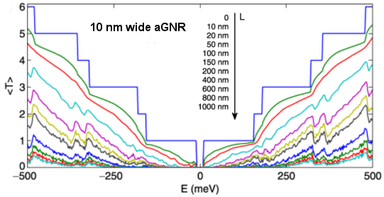 Top: A methyl group grafted on the graphene surface. Bottom: Transmission coefficient, averaged over 50 disorder realizations, as a function of the electron energy for a 10 nm wide armchair ribbon with a density n = 0.1 % of methyl-group adsorbates and for different lengths of the functionalized region from 0 to 1 ?m. |
The absence of band gap is a major issue for the use of graphene in logic devices, whose on/off current ratio turns out to be very poor. Graphene chemical modification is a perspective tool to open a transport gap and design efficient carbon-based logic transistors. Starting from ab initio calibrated tight-binding models, we simulate transport in nanoribbons in the presence, for example, of methyl group functionalization or boron substitutional doping. Varying the density of adsorbates and the system size and geometry allows us to engineer the transport gap. The simulation of a complete boron-doped graphene-based transistor shows that actually screening can partially reduce the expected high on/off current ratio, thus indicating the necessity for a further optimisation (in terms of doping and electrostatics) and to explore the use of different types of dopants |
Contact: Alessandro Cresti
Recent publications:
• A. Cresti, Scaling properties of diffusive electronic transport in graphene nanoribbons functionalized with methyl-groups, J. Comput. Electron. 12, 94 (2013)
• P. Marconcini, A. Cresti, F. Triozon, G. Fiori, B. Biel, Y.-M. Niquet, M. Macucci and S. Roche, Atomistic boron-doped Graphene Field-Effect Transistors: A Route toward Unipolar Characteristics, ACS Nano 6, 7942 (2012)
• S. Roche, B. Biel, A. Cresti and F. Triozon, Chemically enriched graphene-based switching devices: A novel principle driven by impurity-induced quasibond states and quantum coherence, Physica E 44, 960 (2012).
• A. Cresti, A. Lopez-Bezanilla, P. Ordejón and S. Roche, Oxygen surface functionalization of graphene nanoribbons for transport gap engineering, ACS Nano 5, 9271 (2011).
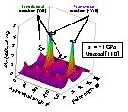
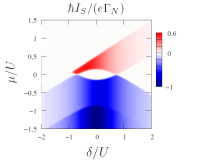
 Density plot of the current injected into the superconducting lead IS in an interacting double dot system as a function of the detuning ?=2?+U, being ? the dot level and U the Coulomb interaction, and of the chemical potential µ of the normal leads for degenerate dots’ levels ??=0. |
We develop a real-time diagrammatic technique to describe non-equilibrium transport through interacting quantum dots connected to normal and superconducting leads. We compute the Josephson current given by the transport of Cooper pairs between the two superconductors and the Andreev current in normal leads. Normal contacts allow us to control the level population and to bring the dot out of equilibrium. |
Contact: Marco Pala
Recent publications:
• A. Braggio, M.G. Pala, M. Governale, J. König, Superconducting proximity effect in interacting quantum dots revealed by shot noise, Solid-State Communications 151, 155, (2011).
• D. J. Eldridge, M.G. Pala, M. Governale, J. König, Superconducting proximity effect in interacting double-dot systems, Physical Review B 82, 184507 (2010).
• D. Futterer, M. Governale, M.G. Pala, and J. König, Nonlocal Andreev transport through an interacting quantum dot, Physical Review B 79, 054505 (2009).
• M. Governale, M.G. Pala, and J. König, Real-time diagrammatic approach to transport through interacting quantum dots with normal and superconducting leads, Physical Review B 78, 069902 (2008).
• M.G. Pala, M. Governale, and J. König, Non-Equilibrium Josephson and Andreev Current through Interacting Quantum Dots, New Journal of Physics 9, 278 (2007).
|
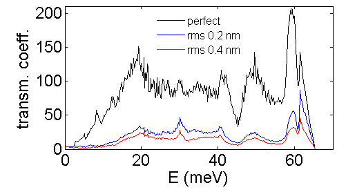
The increasing need for autonomous applications demands the development of efficient energy harvesting techniques, mainly based on thermoelectricity, piezoelectricity or photovoltaic effect. In the last decade, material nanostructuration has allowed a significant increase of the thermoelectric ZT factor of merit thanks to the combined effect of thermal conductivity decrease and moderate impact on the electron conductivity. In our group, we focus on semiconductor nanowires, which have been experimentally seen to be very promising in this respect. We describe the interatomic coupling by a valence force model, which is able to account for experimentally relevant sources of disorder such as roughness, and estimate the thermal conductivity by the Green’s function approach. The combination with electronic transport simulation, for the calculation of conductivity, Seebeck coefficient and electronic thermal conductivity, allows us to estimate the ZT factor and to explore new possible roots for its engineering. lead. |
Contact: Alessandro Cresti , Marco Pala
See for instance: G. Ardila, A. Kaminski-Cachopo, M. Pala, A. Cresti, L. Montes, R. Hinchet, J. Michallon, M. Daanoune, M. Mouis, Towards self-powered systems: using nanostructures to harvest ambient energy, 2nd Ukrainian-French Seminar, April 8-11 2013, Kiev, Ukraine
Date of update November 4, 2019