Aller au menu Aller au contenu
Centre for Radiofrequencies, Optic and Micro-nanoelectronics in the Alps

> Research > CMNE > Modeling and Simulation

Simulation & Modelling-old

Headed by  : Alessandro CRESTI

Context and objectives

Modelling and simulation is a transverse activity inside the “Micro and Nano Electronics Devices” research group. 

The research activity of the modelling and simulation group is devoted to study electron transport of innovative devices such as multi-gate transistors, nanowire FETs, graphene-based devices and mesoscopic structures.
The group has a solid experience in developing homemade numerical codes to solve the 3D/2D/1D self-consistent Poisson-Schrödinger equation with k.p and tight-binding Hamiltonians for accurate band profile calculations and hence to compute electronic and transport properties (LDOS, current density, conductance, mobility). Quantum transport is treated within the general Keldysh-Green’s function formalism, which allows us to take into account non-equilibrium effects elastic scattering due to roughness, charged defects and traps and inelastic interactions such as electron-phonon scattering.
The analytical modelling activity develops physically based analytical models for advance CMOS (Single Gate and Multiple Gates) architectures to improve core models for industrial compact MOSFET models such as PSP and predict MOSFETs performances along the roadmap.

The physical models developed by the group aim at:
  • Predicting and optimising the device performance,
  • Explaining experiments and characterization data
  • Supporting the experimental work performed in the laboratory as the derivation of physically significant parameters from electrical characterisation.

Expertise in modelling

  • Development of physically based analytical models for advance CMOS (Single Gate and Multiple Gates) architectures including:
    Quantum confinement, Quasi Ballistic transport, Strained channels, Leakage currents (Short Channel Effects, Band to Band Tunnelling, Source to Drain Tunnelling),
  • Improvement of core models for industrial compact MOSFET models such as PSP, 
  • Prediction of MOSFETs performances along the roadmap,
  • Transport in Ultra Thin Dielectrics, including High K materials  
  • Modelling of advanced Non Volatile Memory (Flash, Nanocrystal NVM):
    erase and writing time, retention time and reliability
  • Diagrammatic technique for transport properties of the single-electron transistor at different orders of the tunnel-coupling with both normal and superconducting leads 

Expertise in numerical simulation

  • Simulation of quantum transport in nanostructures like semiconductor nanowires, graphene-based structures and mesoscopic devices
  • Resolution of the (3D, 2D, 1D) self-consistent Poisson-Schrödinger equation for accurate band profile calculations
  • Calculation of transport properties (charge or spin) of nanodevices based on the Keldysh-Green's functions approaches with the inclusion of spin-orbit coupling and external magnetic fields
  • Modelling of the effects of elastic scattering due to surface roughness and of inelastic scattering due to phonons
  •   Modelling of heat transport in nanostructures

Impact of mechanical strain on electron and hole transport

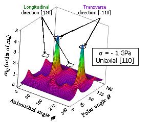
Calculation of the hole conduction mass reduction
due to a longitudinal compressive stress along the
[110] direction. In contrast, the transverse mass
almost keeps its unstrained value.


An analytical model of electron and hole mobility in strained silicon is being developed in order to describe low field transport along any channel orientation with an arbitrary stress configuration (arbitrary stress tensor). The model, which runs in a few seconds on a standard PC, is based on an exact solution of the 6x6 k.p Hamiltonian coupled with a Kubo-Greenwood approach for mobility calculation. It can be used to support the interpretation of experimental results in terms of strain induced mobility variations or to find channel orientations and stress configurations that optimize carrier transport.

Contact: Mireille Mouis
Support: ACI Contraintes (2002-2005), ANR/PNANO MODERN (2005-2008), FP7/IST
See for instance: T. Guillaume, M. Mouis, Calculations of hole mass in [110]-uniaxially strained silicon for the stress engineering of p-MOS transistors, Solid-State Electronics, Volume 50, Issue 4, Pages 701-708 (April 2006)

Simulation of Scanning Gate Microscopy (SGM) experiments: local density of states in mesoscopic structures and manipulation of electron transport


Total wavefunction and conductance maps simulating a Scanning Gate Microscopy (SGM) experiment on a coherent ring. Simulations are obtained with a code based on S-matrix calculations. Under specific conditions, conductance images reproduce the local density of states .


This activity concerns the modelling of advanced SGM experiments on mesoscopic devices like Aharonov-Bohm rings. Scanning gate microscopy is a weakly invasive technique, applicable to nanostructures patterned in subsurface two-dimensional electron gases and operated at low temperature. In such a cryogenic atomic-force-
microscope (AFM) set-up, the probe is used as a scatterer which locally modifies the electron flow properties, or as a local gate which can be moved to any position. We support our interpretation with numerical simulations of quantum transport based on S-matrix or recursive Green's functions approach.

Contact: Marco Pala
Support: Agence National de la Recherche,  « MICATEC » project
Relevant publications:
  •     M.G. Pala, S. Baltazar, P. Liu, H. Sellier, B. Hackens, F. Martins, V. Bayot, X.Wallart, L. Desplanque, S. Huant, Transport inefficiency in branched-out mesoscopic networks : An analog of the Braess paradox, Physical Review Letters 108, 076802 (2012)
  •   B. Hackens, F. Martins, S. Faniel, C. A. Dutu, H. Sellier, S. Huant, M. Pala, L. Desplanque, X. Wallart, V. Bayot, Imaging Coulomb Islands in a Quantum Hall Interferometer, Nature Communications 1, 39 (2010).
  •  M.G. Pala, S. Baltazar, F. Martins et al., Scanning gate microscopy of quantum rings: effects of an external magnetic field and of charged defects, Nanotechnology 20, 264021 (2009).
  •  H. Sellier, S. Huant, B. Hackens, M.G. Pala, Imager les interférences quantiques dans les semi-conducteurs, Images de la physique 2009, Editions CNRS.
  •     M.G. Pala, B. Hackens, F. Martins, H. Sellier, V. Bayot, S. Huant, and T. Ouisse, Local density of states in mesoscopic samples from scanning gate microscopy, Physical Review B 77, 125310 (2008)
  •     F. Martins, B. Hackens, M.G. Pala, et al., Imaging electron wave functions inside open quantum rings, Physical Review Letters 99, 136807 (2007).

Transport gap in chemically modified graphene ribbons

Transport gap in chemically modified graphene ribbons
   
Transport gap in chemically modified graphene ribbons
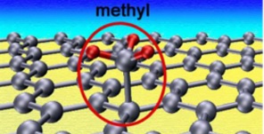
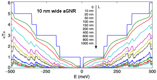
Top: A methyl group grafted on the graphene surface. Bottom: Transmission coefficient, averaged over 50 disorder realizations, as a function of the electron energy for a 10 nm wide armchair ribbon  with a density n = 0.1 % of methyl-group adsorbates and for different lengths of the functionalized region from 0 to 1 ?m.

 The absence of band gap is a major issue for the use of graphene in logic devices, whose on/off current ratio turns out to be very poor. Graphene chemical modification is a perspective tool to open a transport gap and design efficient carbon-based logic transistors. Starting from ab initio calibrated tight-binding models, we simulate transport in nanoribbons in the presence, for example, of methyl group functionalization or boron substitutional doping. Varying the density of adsorbates and the system size and geometry allows us to engineer the transport gap. The simulation of a complete boron-doped graphene-based transistor shows that actually screening can partially reduce the expected high on/off current ratio, thus indicating the necessity for a further optimisation (in terms of doping and electrostatics) and to explore the use of different types of dopants


Contact: Alessandro Cresti
Recent publications:

•    A. Cresti, Scaling properties of diffusive electronic transport in graphene nanoribbons functionalized with methyl-groups, J. Comput. Electron. 12, 94 (2013)
•    P. Marconcini, A. Cresti, F. Triozon, G. Fiori, B. Biel, Y.-M. Niquet, M. Macucci and S. Roche, Atomistic boron-doped Graphene Field-Effect Transistors: A Route toward Unipolar Characteristics, ACS Nano 6, 7942 (2012)
•    S. Roche, B. Biel, A. Cresti and F. Triozon, Chemically enriched graphene-based switching devices: A novel principle driven by impurity-induced quasibond states and quantum coherence, Physica E 44, 960 (2012).
•    A. Cresti, A. Lopez-Bezanilla, P. Ordejón and S. Roche, Oxygen surface functionalization of graphene nanoribbons for transport gap engineering, ACS Nano 5, 9271 (2011).

Andreev and Josephson currents through interacting quantum dots

Andreev and Josephson currents through interacting dots
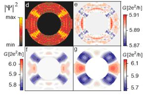
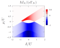
Density plot of the current injected into the superconducting lead IS in an interacting double dot system as a function of the detuning ?=2?+U, being ? the dot level and U the Coulomb interaction, and of the chemical potential µ of the normal leads for degenerate dots’ levels ??=0.

We develop a real-time diagrammatic technique to describe non-equilibrium transport through interacting quantum dots connected to normal and superconducting leads. We compute the Josephson current given by the transport of Cooper pairs between the two superconductors and the Andreev current in normal leads. Normal contacts allow us to control the level population and to bring the dot out of equilibrium.
For a system with two superconducting leads, in the large-superconducting-gap limit, we are able to calculate the non-equilibrium Andreev and Josephson currents to all orders in the tunnel coupling with the superconducting lead.


Contact: Marco Pala
Recent publications:
•    A. Braggio, M.G. Pala, M. Governale, J. König, Superconducting proximity effect in interacting quantum dots revealed by shot noise, Solid-State Communications 151, 155, (2011).
•    D. J. Eldridge, M.G. Pala, M. Governale, J. König, Superconducting proximity effect in interacting double-dot systems, Physical Review B 82, 184507 (2010).
•    D. Futterer, M. Governale, M.G. Pala, and J. König, Nonlocal Andreev transport through an interacting quantum dot, Physical Review B 79, 054505 (2009).
•    M. Governale, M.G. Pala, and J. König, Real-time diagrammatic approach to transport through interacting quantum dots with normal and superconducting leads, Physical Review B 78, 069902 (2008).
•    M.G. Pala, M. Governale, and J. König, Non-Equilibrium Josephson and Andreev Current through Interacting Quantum Dots, New Journal of Physics 9, 278 (2007).

Thermoelectric energy harvesting in semiconductor nanowires

Thermoelectric energy harvesting in semiconductor nanowires
 
 Phonon transmission coefficients for a pristine nanowire and for the two rough nanowires.


Top: Two silicon nanowires oriented along the ‹100› direction, with 5x5 nm2 section and different levels of roughness over a length of 34 nm.
Bottom: Phonon transmission coefficients for a pristine nanowire and for the two rough nanowires.

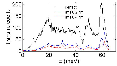
The increasing need for autonomous applications demands the development of efficient energy harvesting techniques, mainly based on thermoelectricity, piezoelectricity or photovoltaic effect. In the last decade, material nanostructuration has allowed a significant increase of the thermoelectric ZT factor of merit thanks to the combined effect of thermal conductivity decrease and moderate impact on the electron conductivity. In our group, we focus on semiconductor nanowires, which have been experimentally seen to be very promising in this respect. We describe the interatomic coupling by a valence force model, which is able to account for experimentally relevant sources of disorder such as roughness, and estimate the thermal conductivity by the Green’s function approach. The combination with electronic transport simulation, for the calculation of conductivity, Seebeck coefficient and electronic thermal conductivity, allows us to estimate the ZT factor and to explore new possible roots for its engineering. lead.


Contact: Alessandro Cresti , Marco Pala
See for instance: G. Ardila, A. Kaminski-Cachopo, M. Pala, A. Cresti, L. Montes, R. Hinchet, J. Michallon, M. Daanoune, M. Mouis, Towards self-powered systems: using nanostructures to harvest ambient energy, 2nd Ukrainian-French Seminar, April 8-11 2013, Kiev, Ukraine

Date of update October 15, 2020

French
CROMA
Grenoble site
Grenoble INP - Minatec : 3, Parvis Louis Néel - CS 50257 - 38016 Grenoble Cedex 1

Chambery site
Université Savoie Mont Blanc - Rue Lac de la Thuile, Bat. 21 - 73370 Le Bourget du Lac
 
 
République Française         Logo CNRS_2019        Logo Grenoble INP - UGA   Grenoble Alps University    Université Savoie Mont Blanc
Université Grenoble Alpes